
There’s no doubt about it. This is a good time to be in the microelectronics and packaging sector of the semiconductor industry. With exciting markets like artificial intelligence (AI), 5G, and the internet of things (IoT) technologies moving from ideas to implementation, this previously tired segment of the semiconductor industry is poised for action and faces abundant opportunities.
“The semiconductor industry is great, because it is confusing, competitive, and greater opportunities always lie ahead. We have AI, even though we don’t really know what it is. We haven’t yet realized the business aspects of the IoT. And 5G will be fantastic.”
With these statements, ASE’s Tien Wu, Ph.D., dove into one of the most inspirational keynote speeches about microelectronics and packaging that I’ve ever heard presented, setting the stage for the 51st IMAPS International Symposium, which took place October 9-11, 2018 Pasadena, CA.
The Tao of Wu
“We see what we choose to see because all perception is a choice,” said Wu, invoking Eastern philosophy. “If we see crisis and dilemma, we address crisis and dilemma. If we see opportunity, we address the opportunity.”
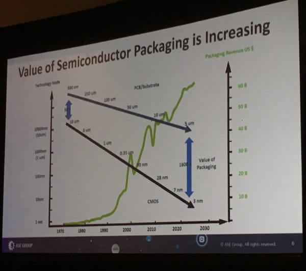
So, while some would tell you that the industry is facing crisis and dilemma with the slowing of Moore’s law; a 1600x gap between lithography and packaging feature sizes (Figure 1) and China tariffs that will impact supplies and leave big question marks on industry growth; from Wu’s perspective, these are merely hiccups that offer great opportunity for the microelectronics and packaging sector of the industry.
A Packaging Love Story
Wu’s career has been one life-long love affair with packaging. He recalls – almost with resentment – the days when front-end manufacturers didn’t see a need for packaging and told packaging engineers to just follow along and figure it out.
“As long as Moore’s law was moving along, we didn’t have to change anything about our approach to packaging,” he says.
Wu also finds it mindboggling that although flip-chip technology was available in 1967, it didn’t become available to the OSATS until 2000, and didn’t become volume viable until 2010. “That’s 30 years of Delta!” he said.
But the pace of adoption has accelerated as the value packaging brings to the entire system has increased.
He cited both TSMC’s investment in integrated fan-out technologies (InFO) to create a viable foundry bridge to fill the 1600x gap, and Deca Technologies’ M-Series as examples of packaging schemes that have had a faster path to implementation.
M-Series, in development for the past 8 years with significant investment by ASE and others, went into volume production at ASE on July 16, with 180M units shipped to date. Wu says ASE expects to ship 25K 300mm M-Series wafers/month. The company is also investing in panel-level M-Series, enabled by Adaptive Patterning™
‘Each panel is equivalent to 5 twelve-inch wafers,” he noted. “We expect extremely high yield and high reliability from that.”
Uplifting Semiconductor Value
What will happen if the packaging industry doesn’t respond to the need for innovation? Wu predicts the gap will widen and Moore’s law will slow down, impacting the entire value of the semiconductor system.
Unlike other technology markets, Wu says Capex is not useful for setting the value of the semiconductor industry. We gain more value through innovation. That is what makes us unique.
Rather than next-generation technology rendering existing technology obsolete, as was the case for LED displays and solar panels, our unique ecosystem has benefited from the cumulative investment of innovation over the years.
“Our waters run deep, and there are many fish at all the levels,” he said. “Today we are still shipping 6- and 8-inch wafers. For many foundries, the 8-inch wafers are still the most profitable.”
Additionally, when we think about improving the value of the semiconductor industry, Wu says we can’t only think about the hardware. Hardware value depreciates. For innovation to be effective we must consider the full scope including firmware and software with the flexibility that allows us to push innovation to the next level.

Ultimately, we have to move architectural designers into a different paradigm to create value for the entire semiconductor supply chain.
The Elephant in the Room
China.
Here’s what Tien Wu had to say:
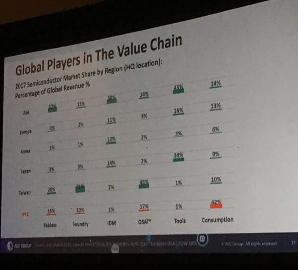
China consumes 42% of semiconductor content while holding only a small percentage of each area of the value chain (Figure 2). The rest of the world complains about China, yet China is the largest consumer of semiconductor content (to the tune of 180B USD/year) while being the smallest producer.
“Is that acceptable for the Chinese?” said Wu “The right thing is for China to have a bigger presence across the board that incrementally approaches the consumption they represent.”
He also doesn’t see China as a threat to the established industry leaders, and that their success won’t come from building the next great tool. For China to gain market share, they must have innovation, he said. He also sees this as an opportunity we can all benefit from.
For example, demand for capacitors to meet needs in automotive, IoT and 5G applications has caused a shortage in supply. Wu says the shortage is also due to the fact that capacitors are a money loser, so no one wants to make them. Here is an opportunity for China to step in and take the lead, he said.
“Whenever we see a new opportunity that the rest of the world doesn’t invest in, we should support China like there’s no tomorrow,” he said.
What about IP?
Wu says IP has always been an issue between companies that are sharing a massive supply chain. Whatever one company invents, the supplier tries to market the same tool to their competitor. The key is finding a way to address innovation differentiation while accepting the basic norm.
Bottom line: Wu says conflict of interest and competition between regions and business entities also present great opportunities for innovation and collaboration.
Summing it Up
Throughout his keynote, Wu touched on different aspects of the ecosystem and their importance to uplifting the value of the semiconductor industry, such as the importance of EDA tools to support a multitude of package designs and forming business alliances to keep up with increasing volumes to support a growing application space.
“Moore’s law will evolve. The packaging community can’t change that,” says Wu, “But we can offer more tools in the toolbox and figure out how to handle any lithography feature or system power demand and put it together with the lowest cost and highest flexibility.”
Wu closed by saying that play-to-win is the only unchanging rule in the “Semi-Jungle.” We say, bring it on.


