
Lots of news over the weekend regarding TSMC. The big news is that TSMC is projected to build its first new fab in the United States since 1998 and have it ready for production in 2024 at the 5nm technology node.
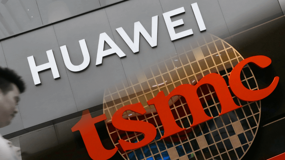
The question I asked myself first, is who is throwing whom a bone; although, with TSMC canceling new Huawei orders, it looks like TSMC is making concessions to the U.S. commerce department.
The next is what are you going to do with a 20,000 wafer starts per month fab? Most TSMC fabs are 50,000 wafer starts per month, and when they complete their mega fabs they typically have 100,000 wafer starts per month capability (wspm).
Dan Gallagher of the Wall Street Journal wrote an article on May 15, that did an excellent job of defining TSMC’s motives in his subtitle:
“TSMC’s new Arizona plant will be limited in scale and expensive to operate but will pay off politically”
The last Fab TSMC built in the USA was in 1998: A 200mm joint venture fab that TSMC eventually bought out. Morris Chang the long-standing CEO of TSMC was often questioned why or when TSMC would build another semiconductor Fab in the USA. His comments from 2017 are below:
Chang cautions that building a plant in the US “may not necessarily be a good thing” for TSMC’s customers and believes that his company is already helping to create jobs in the US because of the products it manufactures and ships to the region. Manufacturing in the US could cause the prices of devices using their chips to increase because of the high US labor costs. The proximity of the current plants to their customers is also an issue that must be considered. It is easier to ship parts, solve issues, and talk to one another when the parts manufacturer is close to the purchaser.“
It has long been rumored that TSMC favored Taiwan, due to labor costs and that young Taiwanese engineers would put in extraordinary hours to help TSMC achieve success.
As Gallagher points out, a 20k wspm fab would potentially be a margin drain on TSMC. It was figured out in the early days of 300mm, when the fabs quickly moved from 20k wspm to 40k through 100k wspm, that economies of scale were needed to help make them more profitable.

So, in what situation would a 20k wspm fab make sense? Gallagher has already pointed out the political necessity. One argument would be that it is to curry favor with the commerce department. But since TSMC just canceled new Huawei orders, which account for a significant amount of revenue, the reason has to be deeper.
A TSMC Military Foundry?
Could it be that the TSMC fab is being designed as a military foundry? With Global Foundries slowing their development path and no longer chasing leading edge, there is no U.S. facility to manufacture leading-edge semiconductor technology for the U.S. government. The Government could possibly turn to Intel, but with companies such as Xilinx designing chips for the Government, this would potentially have some competitive challenges. Military semiconductors typically demand high prices and high margins. Lot sizes are relatively small due to a limited number of semiconductors being needed for the specific application. Building a Government-approved fab could enable TSMC to achieve the margins they typically achieve in their larger fabs, thus making this an economically feasible endeavor.
However, at the moment all of this is speculation. What is known is that TSMC has said they will build a small fab in Arizona. Construction is scheduled to start in 2021, with production in 2024, and the $12 billion in spending to take place through 2029. This would suggest a fairly slow ramp if they are only spending $12 billion over 8 years, which only adds to the question of the motivation of TSMC building in the USA. ~ D. Freeman


