

Continuing our look at key Hybrid Bonding (HB) papers at the recent ECTC 2022 in San Diego, CA.
Applied Materials
Hybrid bonding requires a lot of front-end processing tools, thus you can expect Applied Materials (AMAT) to be an entrant in this technology. In its paper “A Holistic Development Platform for Hybrid Bonding” AMAT Singapore presents a modeling platform for the development of a hybrid bonding process. The platform encompasses (a) dielectric interface interactions, (b) chemical mechanical polishing (CMP), (c) electrical performance, and (d) thermo-mechanical reliability.
As we continue to reduce dimensions, HB becomes more and more important since µbumping such as copper pillar bumping with thermocompression bonding has a limit of 10-20μm pitch, whereas hybrid bonding has been shown to be scalable down to below 1μm pitch. As we know, HB involves the bonding of not only the copper surfaces but also the surrounding dielectric (usually oxide).
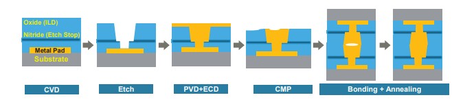
The typical process flow for hybrid bonding is depicted in Figure 1. The metal pad on the last die layer, covered with oxide layers and nitride etch stop, is revealed by etching. Then, the vias are plated through physical vapor deposition (PVD) and electrochemical deposition (ECD) steps. The over-plated Cu is then etched back in a controlled manner using CMP. Finally, the die-to-wafer or wafer-to-wafer hybrid bonding is realized through dielectric bonding followed by annealing.
Dielectric Interface Interactions
Surface activation strongly depends on the ionic and molecular species, which are the products of surface reactions such as plasma treatment and hydration. Due to the complex nature of the applied treatments, most of the surface activation processes require full research of experimental parameters.
Chemical mechanical polishing (CMP)
The key challenges to realizing high-quality hybrid bonding lie in achieving sub-nanometer surface roughness and precisely controlling copper dishing at the bonding surface. A well-controlled CMP process is required to enable shallow and uniform copper dishing. Dishing depth less than 5nm is required to achieve bonding yields greater than 70% at a bonding temperature of 350 C. The dishing dependence on the copper pad pattern was validated as well.
Electrical performance
Electrical modeling of HB interconnects was performed using 3D full-wave electromagnetic simulations to study insertion loss and impedance discontinuities. The impact of misalignment and bump area reduction (arising from the CMP process) were also analyzed. Channel simulations were carried out to understand the impact of process-induced variations on the bandwidth performance of the interconnects.
Electromigration Modeling
Electromigration is the phenomenon where an electrical current through a metallic structure causes the transportation of atoms across the structure. Such a gradual movement of atoms causes voids and hillocks in the structure. These lead to failure since excessive voids increase resistance and eventually burn out, while hillocks may cause shorts. In this study, the current density in the interconnects and traces were predicted using the electrical resistivity of the assigned materials and the electrical boundary conditions. Modeling the electromigration in hybrid bond interconnects helps make decisions on materials and barrier layers, from a reliability perspective. It has been shown that barrier layers such as Ti or Ta alloys, avoid direct contact between copper and the dielectric material, and reduce the magnitude of electromigration.
Tohoku University
Mitsu Koyanagi and his co-workers at Tohoku Univ discussed “Cu-SiO2 Hybrid Bonding Yield Enhancement Through Cu Grain Enlargement”.
Stacked chips in 3D-LSI are electrically interconnected by two key components namely, through-Si-via (TSV) and microbumps (µ-bump). The pitches are in a range of 20 to 40µm for 10-20μm-width µ-bumps. Further scaling of µ-bumps suffers from not only uniform µ-bump electroplating but also from the controlled collapse of µ-bump solder during bonding. To overcome this issue, Cu-to-Cu direct bonding or hybrid bonding technology is gaining greater momentum owing to its ability to form ultra-scaled interconnections (1~2 µm) at much-reduced pitches, below 5 μm. Plasma pre-treatment of the Cu surface and controlling the size and orientation of Cu grains are the two most important strategies to improve the quality and yield of Cu-to-Cu bonding.
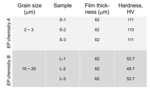
To reduce the Cu-Cu joint resistance, it is highly important to have not only bigger grains but also highly oriented grains (Figure 2).
The lower hardness of the larger grain is expected to result in stronger Cu-Cu direct bonding and Cu-SiO2 hybrid bonding. Shear tests were carried out to determine the Cu-Cu bonding strength. The bonded die with larger grain was nearly 1.25 times stronger than the bond strength obtained for the smaller Cu-grains.
Both Hynix and Samsung made presentations showing the applicability of hybrid bonding to stacked memory.
SK Hynix
Hynix’s presentation was entitled “Wafer to Wafer Hybrid Bonding for DRAM Applications.”

In the DRAM space, there are no commercialized products using the hybrid bonding process so far. Recently, research and development using DRAM are actively underway, so it is expected that DRAM products that apply a hybrid bonding process will come out soon. Existing High Bandwidth Memory (HBM) products formed a stacked structure by connecting chips using micro bumps
This paper described how a stacked DRAM structure was realized by applying the wafer-to-wafer hybrid technology to commercialized DRAM products. The effect on the DRAM characteristics was analyzed, and it was confirmed that the matured DRAM commercialization level was possible by applying Hybrid bonding technology.
The two wafers were bonded using a wafer-to-wafer hybrid bonding process, and then, the substrate Si of the top wafer was ground up to a few μm thicknesses through back-grinding and CMP. All processes in their study used the standard DRAM process.
SiCN was used as the dielectric material rather than SiO2 because it reportedly results in higher bonding strength other than conventional dielectric materials. After deposition of SiCN and patterning of Cu pad, CMP was performed. The amount of dishing or protrusion can be controlled by adjusting pressure and RPM conditions during the CMP process. Conditions were set so that the amount of Cu dishing in the top and bottom wafers was managed to be less than 5nm.
By changing the position of the passivation anneal step and annealing time, it was possible to secure the capacitor characteristics and cell retention characteristics equivalent to the existing mass-produced DRAM.
Hynix reports that due to the robust hybrid bonding connectivity and stable backend metallization process, the final fabricated DRAM product evaluation resulted in the same wafer yields as the existing DRAM products being mass produced. They conclude that “it is expected that wafer-to-wafer Hybrid bonding technology can be applied to various types of 3D integration as they are expanded to DRAM as well as existing NAND.”
Samsung
The Samsung Test and System group discussed “A Study on Memory Stack Process by Hybrid Copper Bonding (HCB) Technology.”
Samsung evaluated hybrid copper bonding (HCB) technology to “overcome a fine pitch limit and degradation in thermal properties in the standard 3D semiconductor package structure.” They successfully demonstrated 3D memory stacking package by HCB technology which integrated Cu-Cu diffusion bonding along with oxide bonding simultaneously. HCB process was developed and a die-to-wafer (D2W) multi-stack structure was realized which shows excellent electrical and thermal properties. The flatness of the bonding surface was controlled by chemical mechanical polishing (CMP), and a highly activated bonding surface was obtained through optimization of plasma conditions. Chip surface properties that were controlled include oxide topography, Cu dishing height, surface hydrophilicity, hydroxyl group density, and adhesion force.
CMP process was optimized to control Cu dishing height variation and topography of the oxide surfaces. Desirable Cu pad dishing height and oxide surface topographies were obtained for oxide-to-oxide bonding and Cu-Cu diffusion bonding. The plasma process conditions were also optimized to modify the bonding surface for better hydrophilicity and higher hydroxyl functional group density. The optimized plasma condition showed the lowest contact angle with the highest hydroxyl functional group density resulting in the highest oxide adhesion force. Finally, the multi-stack HCB process was optimized to acquire a void-free multi-chip stacking D2W structure. Void forming elements were eliminated and defect-free 12-high stacked D2W structures were successfully demonstrated by HCB technology.
For all the latest in Advanced Packaging stay linked to IFTLE…………………………


