
The 72nd IEEE Electronic Components and Technology Conference (ECTC) took place at the end of May in San Diego CA. We all know by now that ECTC is the premier microelectronic packaging conference in the world.

While I was not able to attend in person, it was NOT due to fear of COVID but rather to my granddaughter graduating from high school. Those who have been following IFTLE have watched her grow up since she was 4 years old (see IFTLE 500) and now she has graduated from St Johns in Houston and heads off to Swarthmore College (PA) where she will run track (recall she medaled in the 4 x 400 in the Jr Olympics in 2018). Count IFTLE as one proud grandpa!
Hybrid Bonding Has Made Its Mark
The first thing that stands out when going through the hundreds of papers presented from around the world is that copper-copper hybrid bonding (HB) has made it to the big time. There were more HB papers at this conference than any other topic. It is no longer the interconnect of the future. It now stands on equal footing with solder bumping and copper pillar bumping (C4 and C2 bumping) and you will be seeing it introduced into more and more mainstream products.

Congratulations are due to Paul Enquist and Gil Fountain who worked on the process for 20+ years (mainly at Ziptronix). I retired from the IEEE Electronic Packaging Society Board of Governors after 31 years, but if I were still there, I would be pushing them for the “Exceptional Technical Achievement Award”. If this does not make the cut, nothing should.

I think I can hear Qui-Yi Tong of Research Triangle Institute and Ulrich Gosele, of Max Planck Institute, both now deceased, looking down from above and whispering “I told you so” as this becomes one of the truly important technologies of our generation. Their text, Semiconductor Wafer Bonding: Science and Technology is a seminal work on the topic.
Among them, this group, all working in RTP NC at the time, hold nearly all the key patents and seminal papers on practicing this technology.

In the early 2000s, Ziptronix spun out of RTI as a startup company with technology but no obvious commercial applications. Ziptronix’s extensive patent portfolio was centered around its ZiBond® ( ex. USP 7,387,944) low-temperature oxide process and DBI® (Direct Bond Interconnect) which is now known to the world as Cu-Cu hybrid bonding (ex. USP 6,962,835) technologies. At that time this was a wafer-to-wafer technology. The CMOS image sensor market was the first to see the advantages of this bonding technology. It was Ziptronix CEO, Dan Donabedian who decided to focus on the image sensor market and it was, in hindsight, a brilliant decision.
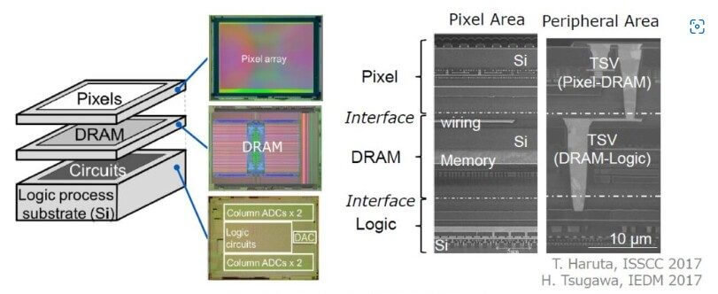
Soon, all the major image sensor manufacturers adopted the Ziptronix technologies. Sony became a major proponent of the technology and as its technology evolved so did its market share. In 2015 Sony commercialized the separation and stacking of the sensor and the circuitry and in 2017 Sony was the first to include DRAM into the stack for its slow-motion capture applications (Figure 5).
For those who think things happen rapidly in the electronics industry, realize this time period of the Ziptronix spin-out to hybrid bonding becoming an accepted interconnect methodology took 20+ years! Having watched it close up, I can tell you it was painful!
As you may recall, Xperi acquired Ziptronix in 2015, about the time when predictions were being made that hybrid bonding could be used to lower the cost of HBM memory stacks. Ziptronix hybrid bonding technology is now part of Adeia, the intellectual property (IP) business of Xperi. (Feature photo)
For a quick technology review, check out the link [ Hybrid Bonding: From Concept to Commercialization ]
Hybrid Bonding at ECTC 2022
IFTLE counts 20+ presentations on hybrid bonding so let’s take a look at a few of them.
Sony
We’ll start with Sony since its CMOS Image Sensor technology led the way. In Sony’s paper Behavior of Bond Strength on Wafer-to-wafer Cu-Cu Hybrid Bonding, they investigated the relationship between misalignment and bond strength before and after copper annealing. Before the annealing process, the bonding strength decreased as the misalignment increased. This changes after the annealing due to the thermal expansion of copper which they discuss in detail.
In their second presentation, Development of Face-to-Face and Face-to-Back Ultra-fine Pitch Cu-Cu Hybrid Bonding, Sony focuses on ultra-fine pitch hybrid bonding which is expected to “drastically improve device performance”. They note that process integration that intentionally fabricates slightly protruded connection pads gives a more robust electrical connectivity for fine pitch Cu-Cu hybrid bonding. This is because the thermal expansion for a 500nm Cu connection pad (corresponds to 1µm pitch) is only 4nm and annealing might not produce a monolithic copper connection without such protrusion.

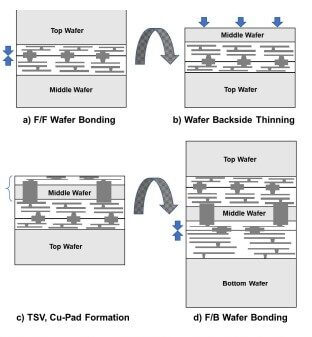
They also reveal that for three wafer stacking, wafer thinning the middle wafer is necessary to lower the difficulty of through silicon via (TSV) fabrication and reduce the total chip thickness. After thinning the middle wafer’s back side, TSVs and Cu connection pads are fabricated and the other side of the Cu connection pads are fabricated on the front side of the bottom wafer. The middle wafer and bottom wafer are thus structurally and electrically connected by face-to-back Cu-Cu hybrid bonding (see below). Overall, they achieve a 1µm pitch for face-to-face bonding and a 1.4µm pitch for face-to-back bonding.
Samsung
Samsung finds that Hybrid Cu bonding (HCB as they call it) results in very large changes in bonding results with small changes in conditions. Therefore, they find the layout design of the chip is very important since even a small design change can change bonding results.
Samsung also looked at the bond pad structure for fine pitch hybrid bonding in its paper A Study on Bonding Pads Structure and Layout for Fine Pitch Hybrid Bonding. Samsung states that compared to micro bump bonding with solder, hybrid bonding can achieve very fine pitch bonding. One of the keys to hybrid bonding is pad processing, which must be optimized for the bonding environment. One must consider Cu expansion at annealing temperature and bonding area between pads because the expansion of Cu pad is proportional to temperature and pad volume. Since annealing temperature is determined depending on the thermal properties of the device, it is important to adjust pad dishing so that connectivity can be secured at the annealing temperature. The initial pad design including pad dishing should be determined by understanding the thermal expansion at process conditions. The amount of Cu extrusion at annealing can be adjusted with an appropriate pad size, or by changing the bonding shape. Therefore, the design rule for fine pad pitch is required based on the relationship between Cu pad surface area and height. When composing the layout, it should be designed in consideration of the surface factors that affect the quality of the initial oxide covalent bonding. In the case of protrusion after annealing, the amount of protrusion can be increased by changing the pad structure, as also noted by Sony.
Samsung also shared its thoughts about voiding at the hybrid bonding interface in the paper Process and Design Optimization for Hybrid Cu Bonding Voids. Unlike conventional solder-based chip bonding, there are various void sources in the gapless hybrid copper bonding process, such as small particles and surface topology, where the interface between the bottom wafer and top chip is in contact without a bonding medium. In addition, the bonding voids have critical risks such as Si popping in the subsequent heat treatment process. Therefore, the control of bonding voids in the development of the hybrid copper bonding process is very important for mass production.
In this presentation, three improvement plans are examined and verified:
The space rule to control the CMP erosion slope – The main cause of erosion, which inevitably occurs due to the nature of the chemical mechanical planarization (CMP) process, is known to be the size and density of patterns in the device. In order to minimize the occurrence of erosion that causes bonding void, it is necessary to understand the pattern-erosion relationship and establish design rules.
The optimization of annealing condition according to a type of oxide film to prevent outgassing – Outgassing may occur at the oxide layer of the interface at high temperatures and increase the risk of Si popping. Therefore, it is necessary to select an oxide film suitable for a high-temperature process or to check the thermal process limit value according to each film type.
The quantitative analysis of voids depending on the property and size of the particle to make a screening spec in the inspection before bonding – In order to understand the relationship between particulate material and the void, the 2D size of the particles was measured by vision inspection just before bonding, and the void size was assessed by after bonding.
(to be continued in IFTLE 529)
For all the latest in Advanced Packaging stay linked to IFTLE………………………


