Hybrid bonding is quickly becoming recognized as the preferred permanent bonding path for forming high-density interconnects in heterogeneous integration applications, from 2DS enhanced, to 3D stacking with or without through silicon vias (TSVs), as well as MEMS and III-V applications. In this exclusive interview with Gill Fountain, Xperi, winner of the 2018 3D InCites Engineer of the Year award for his work in this area, we embark on the journey of how one hybrid bonding technology came to be.
What Do We Mean by Hybrid Bonding?
A quick Google search shows that the semiconductor industry has used the term “hybrid bonding” loosely to refer to any alternative to thermocompression bonding that combines metal interconnect with some other form of bonding. In some cases, it includes adhesives, such as work done by imec and its partners or as presented in this paper by a team from the Dalian University of Technology in China.
In other cases, it involves various interconnect metals such as copper (Cu), indium (In), and silver (AG). One example is solid-liquid inter-diffusion (SLID) developed by Fraunhofer Institute, described in this article by Peter Ramm, Fraunhofer EMFT. Another example is a binary bonding approach that uses InAg combined with atmospheric plasma surface activation, developed by SETNA, described here in this presentation from IWLPC 2015.
For the context of this interview, hybrid bonding is defined as a permanent bond that combines a dielectric bond with embedded metal to form interconnections. It’s become known industry-wide as direct bond interconnect, or DBI (Figure 1).
The early days: developing ZiBond
As Fountain tells it, the DBI story began 20 years ago in the labs at Research Triangle Institute, when his colleague, Paul Enquist, needed a bonding solution that would allow for fine-line lithography after bonding. The pair turned to Q.Y. Tong, described by Fountain as “the leading guru in wafer bonding”, and then manager of RTI’s wafer bonding lab. Together over the next few years, they developed and patented ZiBond, an enhanced version of direct oxide bond that involves wafer-to-wafer processing at low temperatures (150-300degC) to initiate high bond strength rivaling silicon.
“What differentiates ZiBond from other direct oxide bonds? “It’s not just an oxide bond,” explained Fountain. “ZiBond requires the wafer or die surface preparation to be done in such a way that you reach a certain bond strength at a certain temperature.” Exactly what those parameters are is part of the secret sauce. ZiBond is the dielectric bond that forms the basis for DBI.
Ziptronix and the Road to DBI
Armed with the ZiBond patent, Fountain, Enquist, Tong and several other colleagues founded Ziptronix in 2000 as a spin-out of Research Triangle Institute (RTI). What was Fountain’s vision for the company? He gives Enquist all the credit.
“Paul was the guy with the vision. I was just the guy in the lab turning the cranks,” he says. I compared them to Woz and Jobs. He laughs and says, “Paul is a brilliant guy with a lot of good ideas. He has a feel for what would be good for the industry.”
That next vision combined the dielectric bond with embedded metal to simultaneously bond wafers (or die-to-wafer) and form the interconnects.
At the time, the holy grail of 3D stacking was how to stack parts and form the interconnect as part of the bond process at finer pitches than was currently possible using wire bonding. Early prototypes involved cleaning and mounting dies on wafers using ZiBond, and then forming the top connections or through the back of wafer with “brute force” methods to connect bond pad to bond pad. Fountain noted that Sony dabbled in this staple-like approach, but the structures were big. They needed to find a more compact and efficient way to make these connections.
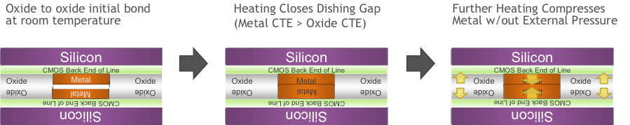
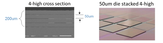
Fast forward to 2005 and the emergence of DBI (Figure 2). The solution was to start with an oxide bond with embedded metal recessed into it. Heat forces the metal together because it expands more than the oxide, causing it to bond, explained Fountain. Initially, nickel was the contact material used because it polished well with oxide, and some are still using it. The first applications to implement DBI were small pitch parts (sub 10µm pitch with 3 µm diameter pads) for focal plane arrays.
Addressing the Challenges
As foundries don’t like to work with nickel, it was important to get Cu to work with the process. The biggest challenge involved surface cleaning and achieving surface topology.
“Adhesives are tolerant of particles,” explained Fountain. “DBI requires particle-free clean surfaces. Additionally, the surface and oxide must be smooth, and the metal has to be slightly below the surface,”
The team figured a few things out along the journey, like what materials worked best for Cu and barrier polish and played around with pushing temperatures as low as possible to expand the process window to more applications, such as memory and compound semiconductors.
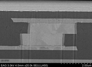
2um pitch Cu DBI wafer to wafer stack (Ziptronix 2011)
“We found that we could readily address engineering challenges associated with cleaning and damascene utilizing the existing equipment sets in foundries today,” noted Fountain. “Damascene copper is their bread and butter. To complete the fabrication process with a surface that can be bonded seems like a natural progression.”

Advantages of DBI
Fountain says DBI overcomes many of the process challenges that plague TCB, such as alignment, and bond strength at tighter pitches. The initial bond forms instantaneously, the alignment of the parts work well, and they don’t slip or move as the bond is strengthened during the low-temperature annealing process. Moreover, the anneal process can be done in batches later, which speeds up the process and improves throughput.
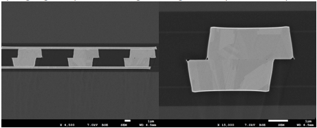
With TCB, parts have to be held in place while heating. DBI is limited only by the alignment capabilities of the bonding tool. 1.5µm pitch is the tightest so far at the die level, but that’s because the tools can’t go smaller, explained Fountain. Moreover, the final bond is stronger because unlike TCB, the bond forms at both the oxide and metal interfaces, not the metal only.
Other approaches to hybrid bonding that call for adhesives or mixed metals don’t form as strong a bond as a single metal, explained Fountain. Adhesives can cause reliability issues due to thermal cycling. Additionally, the bond is hermetic, which positively impacts the reliability of the end device.
DBI’s Journey to Adoption
Despite its elegance, it took a while for DBI to take off. Fountain attributes that mainly to the industry’s resistance to change. Early adopters had a need that wasn’t being met in other ways. For example, Sony was building its image sensors with adhesives and reached distortion limits with lithography.
“We put a lot of work into this technology because we wanted to see it become a useful platform for the industry. It made sense to me that Moore’s law would be expanded by going vertical. Having efficient ways to combine things would be the way of the future,” noted Fountain. “We were a bit ahead of our time, and it took a while to get traction with the technology. But now we are seeing more and more adopters.”
The Journey Continues
Several licenses and an acquisition in 2015 by Tessera Technologies (now Xperi) later, Fountain and his team continue to improve DBI, not only to better understand the polishing processes but to achieve ever-changing device requirements so that it can handle a wide range of applications and pitch sizes.
Most recently, Fountain and his colleagues at Xperi are working on scalable high-volume die-to-wafer bonding, working with different pitch and pad sizes to accommodate high-speed pick-and-place tools that have only 7-9µm alignment accuracy, and a double-sided die preparation process to enable sequential stacking for the memory market. “DBI worked easily at smaller pitches and pad sizes because Cu dishing isn’t an issue. With larger pad sizes it’s more difficult to get appropriate dishing and a flat oxide surface,” explained Fountain. “We’ve expanded the size of pads we can polish to 15-20µm.” Metrology for surface topography check has been key to this development work, he added, crediting his atomic force microscope as the core tool for this work.
The Million Dollar Question
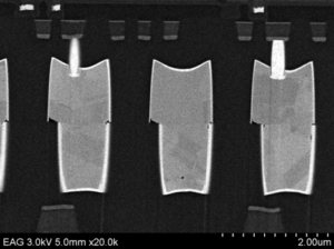
Will DBI become POR across all 3D IC stacking approaches? Fountain is confident that it can and ticked off the reasons why: It’s compatible with foundry processes, and parts can be prepared for bonding right off the line in the fab or OSAT. It can handle fine or large features (Figure 5). Its reliability is good for thermal cycling, high-temperature storage, and high humidity, which is why its suited to automotive applications.
“It’s got a lot of potential. It’s what I’ve known and grown up with my whole career. I have a lot of confidence in it. I’ve seen it do amazing things and have high hopes for its use in the future,” said Fountain. “The fact that a little place in North Carolina could have come up with something that is valuable to a company like Sony just blows my mind.”
Yes indeed. Now I know why Gill Fountain was voted Engineer of the Year. Well done. ~ FvT
This post is the first installment of a new feature, the 3D InCites Winners’ Circle Series, highlighting the winners of the 2018 3D InCites Awards.