
Building integrated circuits (ICs) in the third dimension has been taking place since trench capacitors were introduced for DRAM in the 1980s. The trend continued with the introduction of the damascene process and copper, which quickly grew the back end of the line metallization from 2-3 layers into today’s interconnect skyscrapers, as shown in Figure 1.
The 3D Era in the Front- and Back-ends
FinFETs and 3DNAND further accelerated 3D in the front-end of the line. While the industry is continuing to move forward using 3D technology in the transistor with gate all around (GAA) transistors, then several potential new technologies such as fork sheet transistors and others to move the industry closer to 1nm technology node, and potentially beyond.
The packaging space is where the 3D era is starting to really explode, as technologists have finally figured out how to stack different chips successfully and get them to operate without overheating the package. As a result, the industry is rapidly moving from system in a package (SiP) to 2.5D packaging to 3D packaged systems that are enabling AI and rapidly making 5G edge compute a reality. AMD earlier in the year and then Intel in August have both made announcements with 3D packaged systems that are pushing the industry to much more powerful compute systems that will improve AI and other compute workloads. Let’s step back and look at these recent announcements.
Working with Jim Walker for nearly 15 years, there was frequently the system in package (SiP) Vs. System on chip (SoC) argument. The SiP argument meant putting the chips together in a package, which enabled faster time to market, probably higher yields, and potentially better margins. The downside was slower speeds than the comparable SoC. The SoC argument was a smaller form factor as the components were on the same silicon. A faster chip or system as you didn’t have to deal with chip-to-chip interconnect. The downside was slower time to market and depending upon the technology node, one used lower yields due to a larger die size.
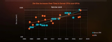
At the 2017 IEDM, Lisa Su, CEO, AMD, presented a keynote talk where the idea of chiplets reemerged. Su advocated that die-size trends were increasing at an unstainable rate (Figure 2). The larger die sizes create both yield issues, as well as process challenges. At that time high bandwidth memory was being used with logic devices using 2.5D packaging to improve system performance. Su stated that the ultimate goal was not only to stack or place DRAM near or on the CPU, but also non-volatile memory, GPU, and other components directly on top of processors.
Since 2017 AMD, TSMC, and Intel have been developing technology that has enabled 3D packaging (Figure 3). AMD using TSMC’s 2.5D and now 3D technology, and Intel implementing their embedded multi-die interconnect (EMIB) and FOVEROS applications to build 3D systems.
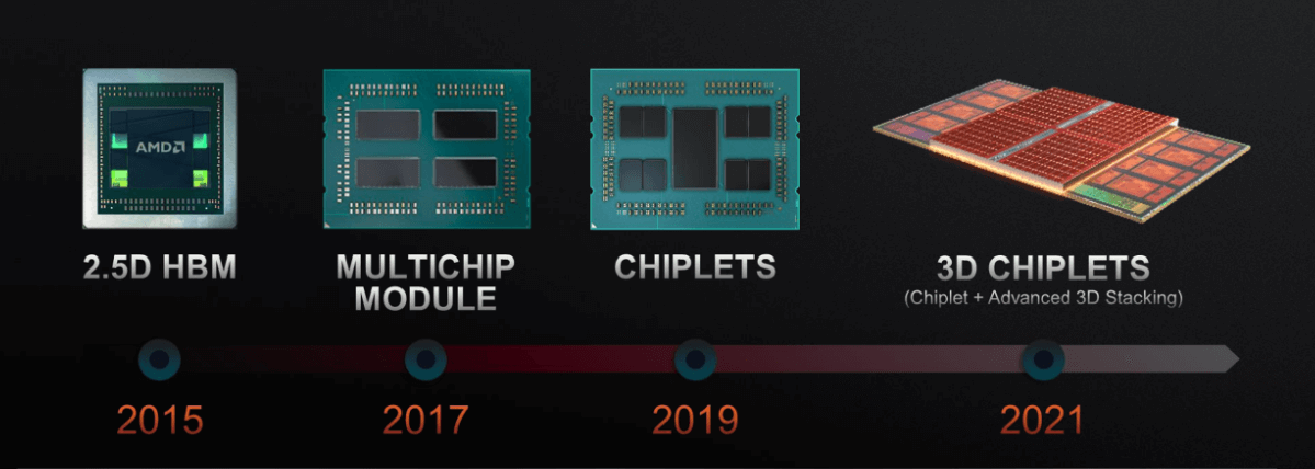
Figure 3: AMD’s 3D packaging roadmap. The company led the pack in HBM, 2.5D, and chiplet architecture, and has an aggressive roadmap for chiplet and 3D integration. (Source AMD Corporate Presentation)
Intel Accelerated
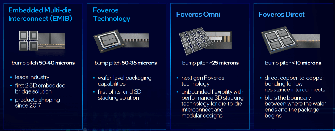
Some keys to making 3D systems a reality have been figuring out how to get the heat out when stacking chips, as well as effective through silicon vias (TSVs), and being able to shrink the bump pitch and increase the bump density. At Intel’s Accelerated Day 2021, Dr. Ann Kelleher, Senior Vice President and General Manager of Technology Development, presented on Intel’s packaging technology (Feature image). Kelleher discussed that the bump pitch would be shrinking from 40-50 microns with the EMIB to less than 10 microns with the Foveros direct process (Figure 3). At Intel’s 2020 Architecture Day, they highlighted that bump density would increase from 330-722 bumps/mm2 to 10,000 bumps/mm2 as the packaging roadmap progressed.
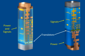
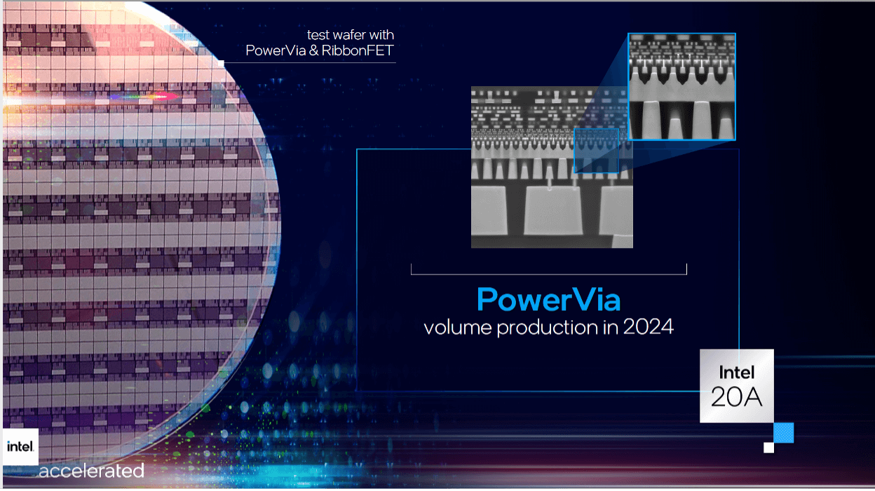
Kelleher and Dr. Sanjay Natarajan, Vice President and Co-general manager of Logic Technology Development, shared further on the technology roadmap. Dr. Mike Mayberry had discussed the need for what Intel is calling “Power Vias” back in October at SEMI’s International Trade Partners Conference, pointing out that power vias can help simplify the interconnect wiring and also help reduce power (Figure 5). IMEC has been on presenting a similar technology they are referring to as a buried power rail.
Kelleher and Natarajan shared that Intel has targeted 2024 and the Intel 20A process node for the introduction of the PowerVia.

New Technology Introductions
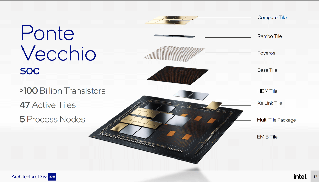
Kelleher then presented on a subject that would then be discussed in great detail on Architecture Day: One of Intel’s new systems the Ponte Vecchio GPU. This is Intel’s first product using EMIB and the second generation of Foveros demonstrating the rapid adoption and implementation of 3D packaging by Intel. The discussion around Ponte Vecchio highlighted the new architectures Intel introduced for I/O, Memory, IP, and SOC, along with new software, verification power delivery, packaging, and other aspects needed to make this processor come together.
One of the holy grails of chiplets or 3D packaging that has been discussed for some time is the ability to incorporate the best of breed chips onto or into the same package. To accomplish this requires industry standards to achieve seamless integration.
Intel closed out Architecture Day by introducing their one API, which is an open standards-based unified software stack. The one API begins to make incorporating different companies’ chips or tiles into the same package, thus enabling customization for a specific compute effort. Figure 8 suggests that competitors’ chips could be placed on or in the same package using Intel’s EMIB or Foveros packaging technology.
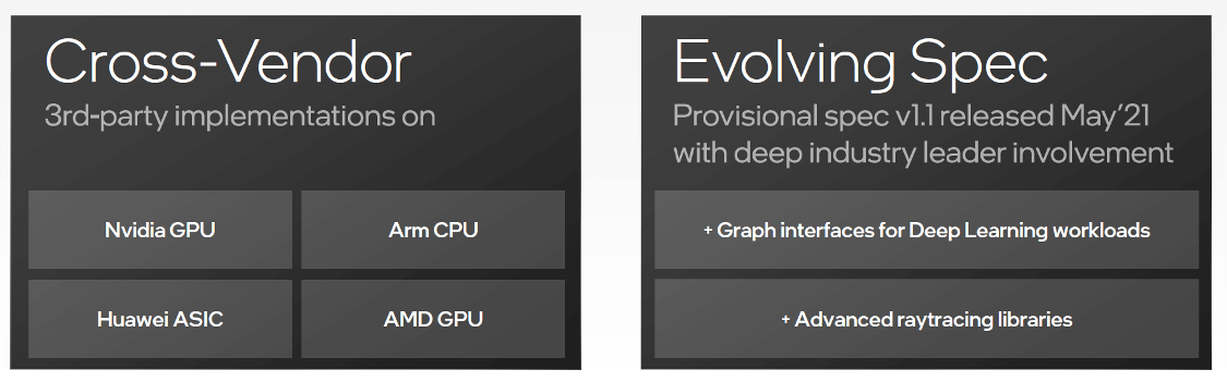
The oneAPI standard has the potential to give the Intel packaging foundry model an interesting marketing angle with which to start business. This also enables companies that are starting to build their own ASICs for AI an opportunity to improve on that chip design by adding in some best-of-breed semiconductor technology at the packaging level to enhance their specific AI application.
Overall this is a good start and more standards will emerge. But for now, the night is still young, and while there is some industry momentum behind the oneAPI, it will likely be a bit before we see competitors’ chips sitting next to each other in the package.


