Koh Young Technology Inc. News

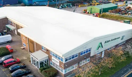
Koh Young America promotes Heriberto Cuevas to Country Manager of its Mexico and South America Operations
Koh Young, the industry leader in True3D™ measurement-based inspection solutions, proudly announces the promotion of Heriberto Cuevas to Country Manager...
Koh Young Webinar to Show How Data Transparency Strengthens SMT Production Resilience
Koh Young, the industry leader in True3D™ measurement-based inspection solutions, invites electronics manufacturing professionals to register for its upcoming webinar,...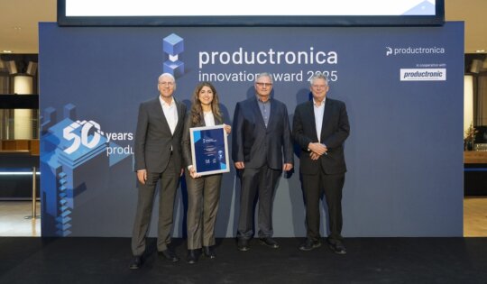
Koh Young Recognized with Productronica Innovation Award for its AI-powered Process Optimization Solution
Koh Young Technology, the global leader in True 3D measurement-based inspection solutions, has been recognized with a Productronica Innovation Award...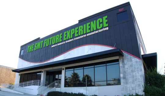
Industry Leaders Koh Young, Fuji America, and Creative Electron Unite to Launch The SMT Future Experience
Three of electronics manufacturing’s most innovative companies announced the formation of THE SMT FUTURE EXPERIENCE, an independent collaborative venue designed...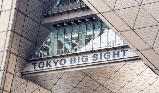
Koh Young Highlights 3D Inspection for Advanced Packaging at SEMICON Japan 2025 in Tokyo Big Sight
Koh Young Technology, the global leader in True 3D measurement-based inspection and metrology solutions, will showcase its latest semiconductor inspection...
Koh Young Technology Appoints Jeff Lee as Head of Industrial Solutions Business
Koh Young Technology, the global leader in True 3D measurement-based inspection and metrology solutions, has appointed Jeff Lee as Head...
Koh Young Unveils Breakthrough Innovations at Productronica and SEMICON Europa 2025
Koh Young, the industry leader in True 3D measurement-based inspection and metrology solutions, will showcase a wave of innovations at...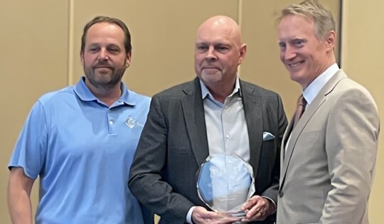
Koh Young Earns Service Excellence Award for the Fourth Time in Five Years
Koh Young Technology, the global leader in True 3D measurement-based inspection solutions, has once again been selected by customers for...
Koh Young Discussing Ways to Apply Smart Factory Insights to Maximizing Productivity at SMTA Tijuana
Koh Young, the industry leader in True 3D measurement-based inspection solutions, will present at the SMTA Tijuana Expo & Tech...
Koh Young to Showcase Semiconductor Metrology and Advanced Packaging Inspection Solutions at IMAPS 2025 in San Diego
Koh Young Technology, the global leader in True 3D measurement-based metrology and inspection solutions, will make its first appearance at...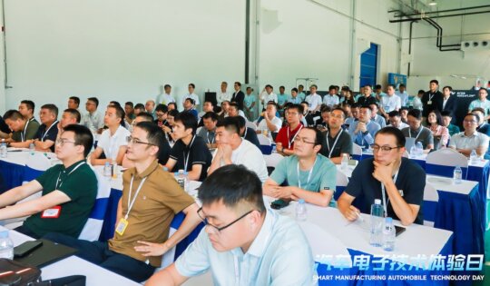
Koh Young, Fuji, and Kurtz ERSA Drive Smart Manufacturing Solutions for EV and Automotive Electronics at Kunshan, China Technical Seminar
Koh Young Technology, the global leader in True 3D measurement-based inspection solutions, partnered with Fuji Corporation and Kurtz ERSA to...
Koh Young Showcases Advanced Dimensional Metrology and Inspection Solutions for Semiconductor and Wafer-Level Packaging at SEMICON West
Koh Young Technology, the industry leader in True 3D™ measurement-based dimensional metrology and inspection solutions, will present its latest advancements...
Koh Young Highlights the Market Driven Nova Series and Smart Factory Solutions at Productronica India 2025
Koh Young, the global leader in True 3D measurement‑based inspection and smart factory platforms, is poised to highlight its cutting‑edge technologies...
Koh Young Hosts First Technical Review Meeting at New Taiwan Office to Showcase Advanced Metrology and Inspection Solutions
Koh Young Technology, the global leader in True 3D measurement-based inspection and metrology solutions, is inviting semiconductor and SMT professionals...
Koh Young Expands Global Footprint with Grand Opening of Taiwan Office to Serve Semiconductor and Advanced Packaging Market
Koh Young Technology, the global leader in True 3D measurement-based inspection and metrology solutions, proudly announces the grand opening of...
Koh Young Highlighting Award-Winning True3D Inspection Solutions at SMTA Guadalajara Expo
Koh Young Technology, the global leader in True 3D measurement-based inspection solutions, will showcase its full portfolio of award‑winning inspection...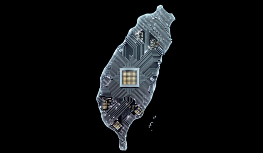
Koh Young Appoints George Hsu to Lead Newly Opened Taiwan Office to Drive Semiconductor and Advanced Packaging Growth
Koh Young Technology, the global leader in True 3D measurement-based inspection and metrology solutions, is pleased to announce the appointment...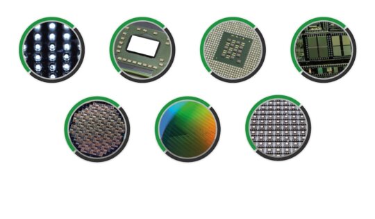
Koh Young Showcases Advanced Dimensional Metrology and Inspection Solutions for Semiconductor and Wafer-Level Packaging at SEMICON India
Koh Young, the industry leader in True 3D™ measurement-based dimensional metrology and inspection solutions, will present its latest advancements for...