SEMICON West 2023 is taking aim at Building a Path Forward with a reimagined exhibition and conference as industry experts and visionaries gather July 11-13 at the Moscone Center in San Francisco. The event focuses on key challenges affecting the global microelectronics industry which include Supply Chain Disruptions, Climate Change, and Talent Shortages, all necessary to enable a $1T industry.
 This year’s SEMICON West is host to several new features that span keynote and conference programming, networking opportunities, and even dining options. Many of our 3D InCites community will be there to connect with the entire extended electronics design and manufacturing supply chain. 3D InCites and SEMI are co-hosting the very first SemiSisters Reception, celebrating all the women who work in the semiconductor industry. Join us from 4-5pm on Tuesday, in the Wine and Beer Garden. Thanks to Edwards for sponsoring this event.
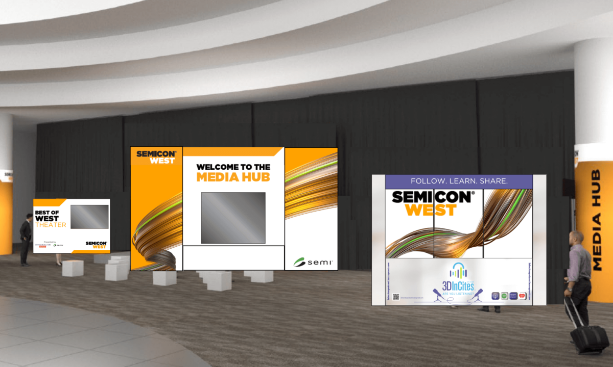
As the official podcast of SEMICON West 2023, Francoise will be onsite recording her “Are You Listening” series, interviewing our member companies and other select speakers from around the industry. Podcast episodes are recorded at the Media Hub, located in the North Hall, by the Best of the West Theater and the Keynote Stage (Figure 1). Please reach out to Francoise directly if you would like to sponsor an episode.
If you missed the SEMICON West Preview interviews with Joe Stockumnas and Tom Sonderman, SkyWater, you can listen to them here.
Here is a small compilation of where our 3D InCites members will be participating and other notable events on the schedule:
Thursday, July 13 | 1:00 pm
New Media Hub, Lower North Lobby
BEST of WEST Stage
Semiconductor Digest and SEMI will present the “BEST OF WEST” awards this year. The award was established to recognize innovative new products moving the semiconductor manufacturing industry forward. Winning entries are products or services that significantly impact the industry as a whole or in a particular application.
MONDAY July 10
3:55 PM – 4:25 PM PDT
The Rise of Automotive Semiconductors – A Packaging Perspective
Location: SF Marriott Marquis, Golden Gate A
Speaker: Prasad Dhond – Amkor Technology
TUESDAY July 11
1:00 PM – 2:00 PM PDT
Navigating Uncertainty-How Do You Build Agile Supply Chains?
Location: Keynote Stage, Room 24, North Lower Lobby
Panelist: Gregory Blanchette – KLA
3:00 PM – 3:25 PM PDT
Building a Better Network: Crucial Conversations
Location: Workforce Development Theater, Moscone North, Exhibition Level, Hall F
Speaker (WFD Pavilion): Antoinette Hamilton – Lam Research
4:20 PM – 4:35 PM PDT
IRAM – Industry4 Readiness Assessment Model a Tool to Guide and Measure progress of your Smart Manufacturing Journey
Location: Smart Manufacturing Meet the Experts Theater, Moscone North, Exhibition Level, Hall F
Speaker: David P. Gross – Siemens
WDNESDAY July 12
10:40 AM – 11:00 AM PDT
Addressing High-Volume Manufacturing Challenges and Technology Inflections in MEMS
Location: TechTalk Stage, Moscone South, Exhibition Level, Room 4
Speaker: Michelle M. Bourke, MBA – Lam Research
11:00 AM – 11:25 AM PDT
Tales from Interns and Recent Graduates
Location: Workforce Development Theater, Moscone North, Exhibition Level, Hall F
Speaker (WFD Pavilion): Cuauhtemoc A. Macias – Lam Research
11:00 AM – 11:20 AM PDT
Pushing the Limits of MEMS Manufacturing
Location: TechTalk Stage, Moscone South, Exhibition Level, Room 4
Speaker: Thomas Uhrmann, PhD – EV Group
11:15 AM – 11:40 AM PDT
Enhanced Parametric Test Insights Through Dynamic Data-Driven Test Flow Execution
Location: Moscone South, Exhibition Level Room 9
Co-Presenter: Greg Prewitt – PDF Solutions
11:35 AM – 11:55 AM PDT
Navigating the Fab in the Metaverse
Location: Smart Manufacturing Meet the Experts Theater, Moscone North, Exhibition Level, Hall F
Speaker: Urmi Sen, MA – Siemens
Speaker: David P. Gross – Siemens
11:30 AM – 11:55 AM PDT
Shaping a Better World Through Microelectronics
Location: Workforce Development Theater, Moscone North, Exhibition Level, Hall F
Speaker (WFD Pavilion): Dara Bobb-Semple, MS, PhD – Lam Research
1:55 PM – 2:20 PM PDT
Quantum and CryoCMOS: Enabling the Future of Computing with Advanced Test & Measurement Tools
Location: Moscone South, Exhibition Level Room 9
Speaker: Jack DeGrave, PhD – FormFactor
Co-Presenter: Brandon W. Boiko, MS – FormFactor
Co-Presenter: Phoenix Dai – FormFactor
2:00 PM – 5:00 PM PDT
Heterogeneous Integration: HPC and Hyperscale Computing – Sponsored by ASE Group
2:00 PM – 2:25 PM PDT
Opportunities from Failure – A Day in the Life of an Engineer
Location: Workforce Development Theater, Moscone North, Exhibition Level, Hall F
Speaker (WFD Pavilion): Theron Smith, PhD – Lam Research
2:45 PM – 3:05 PM PDT
Enabling Smart Manufacturing in Semiconductor Fabs Using Predictive Design and Process Insights
Location: Smart Manufacturing Meet the Experts Theater, Moscone North, Exhibition Level, Hall F
Speaker: Srividya Jayaram, MS – Siemens EDA
3:25 PM – 3:45 PM PDT
Machine Learning Improves Final Test Forecast for Semiconductor Fabs
Location: Smart Manufacturing Meet the Experts Theater, Moscone North, Exhibition Level, Hall F

Speaker: Melvin Lee Wei Heng – ONTO INNOVATION
3:25 PM – 3:45 PM PDT
It’s Better to Trust Each Other
Location: Moscone North, Exhibition Level, Room 21
Speaker: Jason Callahan, MBA, CISSP – Lam Research
4:05 PM – 4:45 PM PDT
Panel: Accelerating Cybersecurity Initiatives
Location: Moscone North, Exhibition Level, Room 21
Panelist: Jason Callahan, MBA, CISSP – Lam Research
THURSDAY July 13
10:00 AM – 10:25 AM PDT
Production Test RF Calibration Methods for Probe Cards
Location: Moscone South, Exhibition Level Room 9
Speaker: Pratik Ghate – FormFactor
10:35 AM – 10:55 AM PDT
Connecting the Dots: From KPIs to Smart Manufacturing Applications to Industry Standards
Location: Smart Manufacturing Meet the Experts Theater, Moscone North, Exhibition Level, Hall F
Speaker: Alan Weber – Cimetrix by PDF Solutions
1:35 PM – 1:55 PM PDT
EUVL Dry Resist for the 1nm Node and Beyond
Location: TechTalk Stage, Moscone South, Exhibition Level, Room 4
Speaker: Benjamin G. Eynon, Jr. – Lam Research
2:25 PM – 2:50 PM PDT
Advancing Probe Card Parallelism for SOC Devices
Location: Moscone South, Exhibition Level Room 9
Speaker: Cameron Harker – FormFactor
Exhibits
Cimetrix by PDF Solutions
- Booth: 344
Cimetrix Incorporated, now part of PDF Solutions, is the leading worldwide provider of equipment connectivity products for smart manufacturing and Industry 4.0. These products reliably and cost-effectively enable manufacturing equipment and factory software systems to connect and communicate over factory networks, providing the necessary model-based data and control capabilities that result in millions of dollars in manufacturing productivity benefits.
Its industry-leading products focus on successful implementation of equipment control and SEMI connectivity standards — SECS/GEM, GEM300, EDA/Interface A, and PV2 — to enable faster time-to-market, lower total cost of ownership, and optimized productivity.
ClassOne Technology
- Booth: 441
Headquartered in Kalispell, Montana, ClassOne Technology has become a preferred provider of advanced wet-chemical wafer processing equipment for ≤200mm semiconductor wafers. The Solstice® series provides high-performance single-wafer electrochemical deposition (ECD) and wafer surface preparation processes. The Solstice platform is available in hardware configurations with two to eight processing chambers to cover process development as well as low-, medium-, and high-volume production. The Trident™ series provides an array of high-efficiency, highly dependable spin-rinse-dryers and spray solvent tools for batch-processing. The company brings high-performance processing technology to compound semiconductor and other key markets, including photonics, power, 5G, microLED and MEMS. Hundreds of ClassOne tools are presently in use building leading-edge devices in major fabs and research facilities around the world.
Edwards
- Booth: M3
Edwards Innovation Lounge @ Semicon West #751
Edwards offers a unique range of equipment solutions, support services and technical expertise to meet sustainability and application needs in the manufacture of microelectronic devices, including silicon and compound semiconductors.
Serving all leading process tool OEMs and with a presence at every major semiconductor fab in the world, its systems are designed to meet the specific requirements of existing and developing processes. A variety of systems, such as dry vacuum pumps, turbomolecular pumps and point-of-use abatement systems are offered to optimise performance across the range of applications, from light duty to the heaviest duty processes.
EV Group Inc.
- Booth: 1235
EV Group (EVG) is a leading supplier of equipment and process solutions for the manufacture of semiconductors, microelectromechanical systems (MEMS), compound semiconductors, power devices, and nanotechnology devices. Key products include wafer bonding, thin-wafer processing, lithography/nanoimprint lithography (NIL) and metrology equipment, as well as photoresist coaters, cleaners and inspection systems. Founded in 1980, EV Group services and supports an elaborate network of global customers and partners all over the world.
Evatec AG
- Booth: 1060
Evatec delivers complete thin film production solutions for advanced packaging, semiconductor, optoelectronics and photonics. Choose from a range of batch, cluster and inline platform architectures for deposition of metals, TCOs, piezoelectrics, dielectrics, magnetics and a whole range of compounds. At this year’s Semicon find out how its new generation CLUSTERLINE helps “power ahead” in thin film processes for power applications on Si, SiC and GaN, and learn how new automated BAK evaporation solutions drive your process quality and throughput up and your cost of ownership down for mass production processes in application areas like Wireless and Optoelectronics.
KLA Corporation (SPTS Division)
- Booth: 829 & 835
KLA develops industry-leading equipment and services that enable innovation throughout the electronics industry. We provide advanced process control and process-enabling solutions for manufacturing wafers and reticles, integrated circuits, packaging, printed circuit boards and flat panel displays. In close collaboration with leading customers across the globe, our expert teams of physicists, engineers, data scientists and problem-solvers design solutions that move the world forward.
SPTS Technologies, a KLA company, designs, manufactures, sells, and supports advanced etch, PVD, CVD and MVD wafer processing equipment and solutions for the global semiconductor and micro-device industries, with focus on the Advanced Packaging, MEMS, high speed RF device, power management and photonics markets. The SPTS Division has manufacturing facilities in Newport, Wales and Allentown, Pennsylvania, and operates across 19 countries in Europe, North America and Asia-Pacific.
Koh Young Technology Inc.
- Booth: 329
Koh Young Technology, a leading provider of 3D Solder Paste Inspection (SPI) and 3D Automated Optical Inspection (AOI) systems, specializes in the design and manufacturing of 3D measurement and inspection equipment for the global circuit board assembly and semiconductor markets. Direct sales and support centers are located in the United States, Europe (Germany), Japan, Singapore, China (Shenzhen) and Korea.
Lam Research Corporation
- Booth: W4
As a trusted, collaborative partner to the world’s leading semiconductor companies, Lam is a fundamental enabler of the silicon roadmap. Its innovative wafer fabrication equipment and services allow chipmakers to build smaller, faster, and better performing devices. We combine superior systems engineering, technology leadership, a strong values-based culture, and unwavering commitment to customer success to accelerate innovation, enabling our customers to shape the future.
MRSI Systems
- Booth: 762
MRSI Systems (part of Mycronic Group) based in Massachusetts, is the leading manufacturer of fully automated, high-speed, high-precision, and flexible eutectic and epoxy die bonding systems. Its solutions span research and development, low-to-medium volume production, and high-volume manufacturing of photonic devices such as lasers, detectors, modulators, AOCs, WDM/EML TO-Cans, Optical transceivers, LiDAR, VR/AR, sensors, silicon photonics, co-packaging optics, 3-D hybrid packaging, and optical imaging products. With 35+ years of industry experience and its worldwide local technical support team, MRSI provides the most effective systems and assembly solutions for all packaging levels including chip-on-wafer (CoW), chip-on-carrier (CoC), PCB, and gold-box packaging.
Nordson TEST & INSPECTION
- Booth: 964
Nordson TEST & INSPECTION offers its customers a robust product portfolio, including Acoustic, Optical, Manual and Automated X-ray Inspection, X-ray Component Counting, as well as Wireless Measurement sensors for front-end semiconductor tool set-up and maintenance. Nordson TEST & INSPECTION is uniquely positioned to serve its customers with best-in-class precision technologies, passionate sales and support teams, global reach, and unmatched consultative applications expertise.
Onto Innovation
- Booth: 629
Onto Innovation is a leader in process control, combining global scale with an expanded portfolio of leading-edge technologies that include: Un-patterned wafer quality; 3D metrology spanning chip features from nanometer scale transistors to large die interconnects; macro defect inspection of wafers and packages; metal interconnect composition; factory analytics; and lithography for advanced semiconductor packaging. The breadth of offerings across the entire semiconductor value chain combined with its connected thinking approach results in a unique perspective to help solve customers’ most difficult yield, device performance, quality, and reliability issues. Onto Innovation strives to optimize customers’ critical path of progress by making them smarter, faster and more efficient. With headquarters and manufacturing in the U.S., Onto Innovation supports customers with a worldwide sales and service organization.
Plan Optik AG
- Booth: 229
Plan Optik AG is the leading manufacturer of structured wafers when it comes to technology. In sectors such as consumer electronics, automotive, aerospace, chemistry and pharmaceuticals these wafers are essential components used as active elements for numerous applications in MEMS technology. The wafers of glass, glass-silicon compounds or quartz are available in sizes up to 300 mm diameter. Wafers by Plan Optik provide high-precision surfaces. Plan Optik wafers are available to minimum tolerances with application-specific structuring and complex material combinations.
Plan Optik AG’s extensive experience in the integration of optical, electronic or chemical functions within a wafer as the basis of MEMS applications has made the company the preferred partner of large international manufacturers. Based on Plan Optik’s expert knowledge the wafers are developed in collaboration with customers such as OSRAM, Infineon, Motorola, Samsung, Honeywell and Bosch.
Siemens Industry Inc
- Booth: 1544
OEMs and Semiconductor Equipment manufacturers are facing tremendous challenges, because electrical devices enter the market within very short intervals of time. A separate line usually has to be built for each product and then dismantled again after short production cycles. Semiconductor Equipment manufacturers not only need to be able to deliver their new machines in a very short period of time, they also have to be able to quickly adapt them to short-term changes. The commissioning phase of machines and lines as well as changing from manual to automated production both offer the potential to save a significant amount of time, and to meet challenging time constraints of electronics companies. Siemens provides an ideal range of automation and digitalization solutions that can be used to create a digital twin of the machine. It helps to develop new machines and lines faster and more flexibly.
SurplusGLOBAL, Inc.
- Booth: 1451
SurplusGLBOAL Inc, one of the largest secondary semiconductor equipment traders with proven track records worldwide and currently have several hundreds of equipment in our inventory. www.SurplusGLOBAL.com Service: Secondary Equipment Trading Reconfiguration Refurbishment Remarketing/Auction Rental Valuation Main Items: Front-End Semiconductor Thin Film PVD, CVD Diffusion Furnace, implanter Photo Stepper, Scanner, Coater, Developer Etch Echer, Asher, CMP Wet Wet Bench Metrology CD-SEM, Surfscan, Overlay, Wafer inspection Back-End Semiconductor: ATE: 1.Memory Tester, LCD Driver Tester, SOC Tester, Logic tester, Handler, Prober, 2.Laser repair system Package: 1.Wire bonder, Die Bonder, Dicing saw, Back grinder, Flip chip Bonder SMT: 1.Chip mounter, Screen Printer, Reflow, Auto inserter, Inspection Equipment
Veeco Instruments, Inc.
- Booth: 1533
Veeco (NASDAQ: VECO) is an innovative manufacturer of semiconductor process equipment. Our proven ion beam, laser annealing, lithography, MOCVD, and single wafer etch & clean technologies play an integral role in the fabrication and packaging of advanced semiconductor devices. With equipment designed to optimize performance, yield and cost of ownership, Veeco holds leading technology positions in the markets we serve.
Yield Engineering Systems, Inc.
- Booth: 1335
YES is a leading provider of technology solutions and process equipment for the Semiconductor Ecosystem & “More than Moore” applications. YES is a provider of surface and materials enhancement technology solutions. YES’s high-tech process equipment helps bring to life complex processes that enable state-of-the-art hardware for emerging Artificial Intelligence (AI), High Performance Computing (HPC), Power Semiconductors, Life Sciences, and Mixed Reality applications. YES’s highly advanced thermal processing systems, deposition systems, and wet etch and clean technologies play a vital role in the processing of legacy & advanced node silicon wafers, next-generation substrates, wafer and panel level packages, compound semiconductors, Internet of Things (IoT) devices, microLED & miniLED displays, and micro-fluidic consumables for genomics.