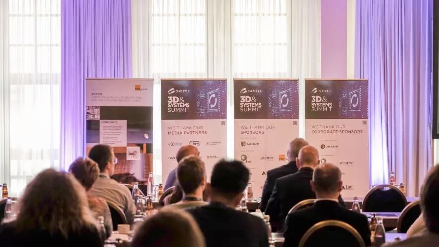
SEMI 3D & Systems Summit to Spotlight Latest Trends in Heterogeneous Integration, Hybrid Bonding, Chiplet Design and Photonics
Leading experts in 3D integration and systems for semiconductor manufacturing will gather at the annual SEMI 3D & Systems Summit, next week June 26-28, 2023 in Dresden, for insights into the latest heterogeneous integration innovations for semiconductor applications enabling the future of intelligent systems. Our own 3D InCites community member companies specialized in 3D integration microelectronics manufacturing will be showcasing their latest products and technologies in addition to speaking in a number of the sessions. Here’s a quick preview where to find them.
DAY 1 | Monday, June 26
5:25 pm – 5:45 pm
Session1 Market Briefing and Technical Roadmaps
5:45 pm – 6:45 pm
Panel Discussion: Customer-Supplier Partnering to Overcome Challenges in 3D

Jan Vardaman
President
TechSearch International, Inc
DAY 2 | Tuesday, June 27
Session 2 Industrialization and Mass Adoption of 3D Technologies
9:05 am – 9:25 am
The Growth of Heterogeneous Integration and Evolution of 3D Packaging

Rozalia Beica
VP Strategic Marketing & Business Development, Microelectronics Business Unit
AT&S China
Session 3 Hybrid Bonding Developments
10:55 am – 11:00 am
Opening Remarks

Thomas Uhrmann
Director of Business Development
EV Group
11:20 am – 11:50 am
PECVD Dielectrics for Inter-die Gap Fill and High Sensitivity Inspection Needs for D2W Hybrid Bonding

Keith Buchanan
Senior Product Manager, PECVD
KLA Corporation (SPTS Division)

Wing-Shan Ribi Leung
Senior Manager of Operations and Applications
KLA Corporation (LS-SWIFT Division)
11:50 am – 12:10 pm
Optimization of the Cu Microstructure to Improve Copper-to-Copper Direct Bonding for 3D Integration

Ralf Schmidt
R&D Manager Semiconductor
MKS-Atotech
Session 4 Chiplet Design Packaging: Architectures and Challenging
2:20 pm – 2:40 pm
Aligning Process Technology, Design, and Architecture for Heterogeneous Integration


Seung Kang
Vice President of Strategy
Adeia, Inc.
3:10 pm – 3:30 pm
Enabling a Chiplet Ecosystem: Standardization of Heterogenous Integrated Chiplet Models

Heiko Dudek
Business Development
Siemens EDA
Session 6: Novel Processes and Interconnect Solutions for 3D
9:50 am – 10:10 am
Nanocleave – Enabling Next Generation 3D Integration

Markus Wimplinger
Corporate Technology Development and IP Director
EV Group
10:45 am – 11:05 am
Thin Film Technology for Heat Dissipation Layers in High-Performance Computing Applications

Roland Rettenmeier
Product Marketing and Business Development
Evatec
Community Member Booths:
Evatec Booth 3
From Semiconductors to Optoelectronics Evatec provides PVD production solutions combining best-in-class cost of ownership with technology innovations to meet future market requirements. Within Advanced Packaging, wafer platforms like HEXAGON and CLUSTERLINE® 300 process wafer up to 300mm whilst the CLUSTERLINE® 600 platform processes substrates up to 650×650 mm. Backside metallization processes enable heat dissipation for High-Performance Computing packages required for Artificial Intelligence (AI) and other intense applications. Evatec’s well-aligned process technologies for degassing, etching, and sputtering ensure the lowest Rc, excellent layer adhesion, and superior film uniformity for Fan-Out and Bumping products.
Website – evatecnet.com
Koh Young Europe GmbH Booth 7
Koh Young Technology Inc., a leading 3D measurement-based inspection equipment and solutions provider performs an essential role in quality control and process optimization in the production fields of diversified industries including automotive, telecommunications, and semiconductors. The company has released the MEISTER product family, a portfolio of True 3DTM Inspection Solutions for solder paste, printed bumps, and solder balls as well as small components like 0201Ms and highly reflective die. With those solutions, it is possible to inspect SiP, FCBGA, FOWLP/FOPLP, and WLCSP packages with high UPH (Unit per Hour).
Website – kohyoung.com
ERS electronic GmbH Booth 12
ERS electronic GmbH, based in the Munich suburb of Germering, has been providing innovative thermal management solutions to the semiconductor industry for more than 50 years. The company has gained an outstanding reputation, notably with its fast and accurate air cooling-based thermal chuck systems for test temperatures ranging from -65 °C to +550 °C for analytical, parameter-related, and manufacturing probing. In 2008, ERS extended its expertise to the Advanced Packaging market. Today, their fully automatic and manual debonding and warpage adjust systems can be found on the production floors of most semiconductor manufacturers and OSATs worldwide.
Website – www.ers-gmbh.com
LPKF Laser & Electronics AG Booth 17
LPKF is a leading provider of laser-based solutions for the technology industry. Our laser systems are critical to the manufacture of printed circuit boards, microchips, automotive parts, solar panels and many other components.
Our customers use our machines to manufacture smaller and more precise components. At the same time, they can increase the functionality of these components and use new design possibilities. This results in products at the forefront of what is technologically feasible, both for industry and for consumers.
Our employees are experts in the field of laser technology and know how to integrate the laser as a tool into powerful machines. As a result, we have a significant impact on progress in a number of high-tech areas. The result is more powerful, smaller and more energy-efficient products and with them improvements in mobility, connectivity, power generation and digital entertainment.
Website – www.lpkf.com
Adeia Inc. Booth 21
Adeia Inc. invents, develops and licenses fundamental innovations that shape the way millions of people explore and experience entertainment and enhance billions of devices in an increasingly connected world. Leveraging the combination of highly experienced technologists, scientists, engineers and advanced R&D labs in San Jose, California and Raleigh, North Carolina, Adeia develops industry-leading 3D integration solutions such as hybrid bonding that meet the demand for greater functionality, higher performance and smaller size for next generation electronics.
Website – www.adeia.com
ASE Global Booth 22
ASE (Advanced Semiconductor Engineering, Inc), a member of ASE Technology Holdings (NYSE:ASX) is one of the world’s largest providers of outsourced semiconductor manufacturing services in assembly and test (OSAT), and, a leading provider of electronic manufacturing services (EMS) through its sister company, USI. Addressing global proliferation of sophisticated electronics geared towards improving lifestyle and efficiency, ASE is strategically integrating synergies between its well established OSAT and EMS business units. ASE is at the forefront of a new class of EMS that delivers modularized, miniaturized ICs with system-level precision to enable high-performance and highly integrated devices. As a result, ASE is truly bridging the gap between silicon and system makers. From traditional semiconductor players to players innovating applications within IoT, wearables, automotive, AR/VR, connectivity and many more, success within an increasingly dynamic market hinges on creating and sustaining highly productive manufacturing partnerships. ASE has proven ability to collaborate closely with customers, to understand markets and create value propositions, and to deliver advanced packaging and SiP solutions to meet growth momentum across a broad range of end markets. Manufacturing facilities are strategically located within key electronics manufacturing hubs, including Taiwan, China, Korea, Japan, Malaysia, and Singapore. Serving customers across the global electronics ecosystem, regional sales offices are located in Sunnyvale (USA), Brussels (Europe), Hsinchu (Taiwan), Shanghai/Beijing (China), Shenzhen (China), Yokohama (Japan), Gyeonggi-do (Korea) and Singapore.
Website – www.aseglobal.com