The semiconductor industry finds itself at a critical juncture, where the traditional paradigms of Moore’s Law are encountering fundamental physical and economic limitations.
As the industry grapples with the imperative to sustain innovation and meet the escalating performance demands of contemporary computing applications, the transition to 3D IC design emerges not merely as a technological evolution but as a profound shift in semiconductor design and integration methodologies. This transformative period necessitates a comprehensive re-evaluation of existing design workflows and fosters unprecedented levels of collaboration across the entire semiconductor ecosystem.
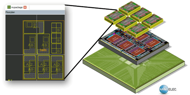
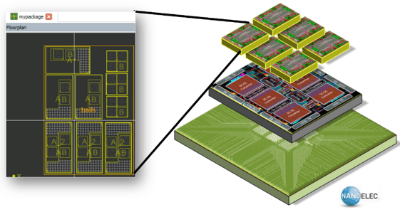
Figure 1. Arrayed blocks are used to construct a chiplet.
Bridging the gap between current design practices and the requirements of 3D IC heterogeneous integration, this article offers a roadmap for both engineering teams and strategic decision-makers navigating the complex 3D IC terrain.
Where 3D IC Stands Today
The term 3D IC is frequently employed broadly within the industry, often encompassing a spectrum of advanced packaging technologies. However, a more precise understanding of the distinction between 2.5D and true 3D integration is paramount for effective design and implementation. The majority of current high-volume implementations utilize 2.5D technology, characterized by the placement of multiple dies side-by-side on a silicon interposer, which in turn is mounted on an organic substrate. This approach has proven highly effective for numerous applications, offering significant performance and bandwidth improvements over traditional 2D packaging, but it represents merely the initial phase of the full potential of vertical integration.
True 3D integration, which is now emerging in new design starts, involves the direct stacking and direct integration of dies on top of one another. This advanced form of heterogeneous integration primarily leverages hybrid bonding technology, enabling ultra-fine pitch connections and significantly higher interconnect densities. These cutting-edge designs often incorporate multi-die stacks interconnected through sophisticated technologies, delivering enhanced performance capabilities and moving beyond the planar constraints of 2.5D.
When it comes to true 3D IC, the semiconductor industry currently takes two paths. At the vanguard, hyperscale cloud providers and major data center operators aggressively push the boundaries of 3D IC technology, particularly in the domains of high-performance computing and AI acceleration. These industry leaders actively deploy advanced integration techniques to leverage the inherent advantages of 3D design.
However, when considering the broader market, 3D IC adoption remains on a slower path. While leading silicon foundries have established mature methodologies, many OSAT providers have similar 3D technologies but struggle with the enablement component. Consequently, there is a discernible variability in the levels of design enablement observed across the industry, with a primary focus currently on design rule checking for physical verification.
In the context of chiplet integration, the vision of a “mix-and-match,” LEGO®-like approach is showing encouraging signs of realization. The increasing adoption of the Universal Chiplet Interconnect Express (UCIe) interface standard is enabling the integration of diverse chiplets beyond traditional memory and computing components. Furthermore, the emergence of specialized chiplets from IP providers is significantly accelerating the general adoption of chiplet-based designs by offering pre-verified, high-performance building blocks.
Economics and Technology Drive 3D IC
The escalating costs and inherent risks associated with advanced process nodes are significant economic drivers. Non-recurring engineering costs for leading-edge nodes can easily exceed $500 million, and the associated risks of design errors and yield issues at these advanced nodes makes the road even bumpier.
From a technical perspective, a critical driver for 3D IC adoption is the imperative for high-bandwidth, low-latency memory access. Hyperscale and edge compute applications, in particular, demand vast amounts of data to be processed with minimal delay. The ability to place memory in close proximity to compute elements through 3D integration significantly alleviates the “memory wall” bottleneck, enhancing overall system performance.
The inherent limitations of traditional monolithic chip design also serve as a crucial tipping point for 3D IC adoption. Reticle size constraints, dictated by the maximum exposure area of lithography tools, make it impractical and often impossible to fabricate extremely large, single-die SoCs. Fabricating exceptionally large dies introduces significant and often prohibitive yield challenges,
Consequently, it has become more cost-effective and yield-efficient to fabricate smaller, functionally optimized chips and then integrate them using 3D IC technologies. This strategy is particularly advantageous when many IP blocks within a complex system do not benefit from the most advanced and expensive process node scaling. By segregating these blocks into separate chiplets and integrating them vertically, designers can optimize the process technology for each component, leading to a more efficient and cost-effective overall system. The “right-sizing” of the process node to the IP is a hallmark of current 3D IC design starts, where compute cores are fabricated at advanced nodes and then integrated with other components via hybrid bonding and advanced substrates.
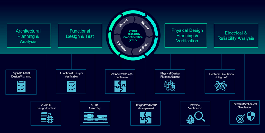
Figure 2. System Technology Co-Optimization facilitates concurrent design work while improving processes for each design fragment..
The demand for high-bandwidth, low-latency memory access has become a primary technical driver for 3D IC adoption. Thus, modern designs frequently incorporate multiple high-bandwidth memory (HBM) stacks, with designs frequently integrating four to eight, even up to 16, HBM stacks — a trend that is expected to continue this upward trajectory.
Data-intensive applications, prevalent in AI, machine learning, and high-performance computing, require even more HBM stacks. The transition to HBM4, expected in 2026, will double the data interface width to 2048 bits and boosts per-pin speeds to 8 Gb/s or higher, resulting in a total bandwidth that is at least double that of HBM3.
This trend underscores the critical role of memory proximity. The integration of HBM inherently requires an interposer-type substrate to accommodate the diverse bump geometries and fine-pitch interconnections associated with these technologies, further solidifying the need for advanced packaging.
Making Change Is Good
The successful transition to 3D IC design requires fundamental transformations in both design methodologies and organizational structures. The traditional “over-the-wall” approach is no longer tenable. Instead, a highly integrated, collaborative, and system-centric process is imperative. This paradigm shift necessitates early consideration of system-level issues, ranging from power delivery networks to thermal management, and demands continuous coordination throughout the entire design flow, from early architectural exploration to final sign-off.
The rapid pace of innovation in advanced packaging itself, with new substrate technologies and assembly formats constantly emerging, presents a continuous challenge for the industry to keep pace.

Hyperscale companies are leading the charge in advanced 3D IC packaging, actively adapting to and influencing these evolving technologies. However, even these pioneers encounter new challenges in 3D verification, power delivery, and thermal modeling, all of which necessitate the development of novel approaches, methodologies, and EDA tools.
For newcomers to 3D IC design, the complexity can be daunting. The initial challenge lies in aligning their application’s performance requirements with an appropriate and cost-effective 3D IC technology that is accessible for volume manufacturing.
Subsequently, navigating the ecosystem, which often involves multiple foundries, OSATs, and other suppliers, each with varying levels of design support and enablement, becomes a significant hurdle. Any gaps in support typically fall to the customer to resolve, underscoring the need for new methods, tools, and a more holistic restructuring to foster a more integrated design environment.
A pivotal methodological shift required is the adoption of a system-centric perspective from the earliest stages of design. This involves early floor planning and continuous system-level analysis through to the final sign-off. Critical questions, such as how power is delivered to the uppermost dies in a stack or how to ensure correct connectivity across multiple stacked components, must be addressed proactively. A holistic understanding of how individual dies, interposers, bridges, and package substrates interact is essential. This includes understanding stacking configurations, placement strategies, and the characteristics of interface layers.
This complexity is further exacerbated by the need to balance conflicting requirements and interdependencies. A prime example is the intricate trade-off between thermal considerations and signal insertion loss. Thermal management is a paramount concern for 3D ICs due to the high power densities and reduced surface area for heat dissipation. Engineers must understand the thermal impact as early as possible, as it drives decisions regarding device spacing, cooling requirements, and overall system architecture.
Striking the optimal balance between these competing requirements necessitates early predictive modeling. This involves adapting downstream modeling tools for use in early design phases to enable rapid evaluation of multiple design scenarios, empowering engineers to make informed decisions that are optimized for thermal, electrical, and mechanical performance.
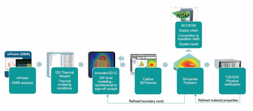
Figure 3. Siemens thermal solutions for 3D ICs.
Beyond methodological changes, an organizational transformation is equally critical. The traditional siloed engineering teams, where chip, package, and system design are treated as distinct, “over-the-wall” processes, are ill-suited for the intricacies of 3D IC. Successful 3D IC design demands a highly integrated, multidisciplinary team with expertise spanning signal integrity, power integrity, thermal analysis, physical layout, and verification. The boundaries between chip and package are increasingly blurred, making a collaborative, holistic approach indispensable.
Siemens plays a pivotal role in facilitating the industry’s evolution towards 3D IC integration by deeply understanding current and future customer needs and partnering to develop high-value solutions. Siemens leverages its extensive portfolio of technologies, encompassing not only established product lines, like Calibre, Innovater3D IC, and Xpedition, but also strategic partnerships and acquisitions. For example, collaborations with IP providers like Alpha Wave bring critical IP solutions, while recent acquisitions, such as Altair, expand capabilities in multiphysics modeling, which is essential for comprehensive 3D IC analysis.
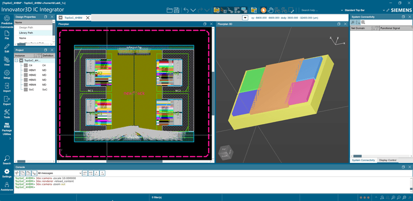
Figure 4. Innovator3D IC solution suite cockpit.
This Way the Future
The successful realization of 3D IC design’s full potential hinges on the availability of comprehensive EDA toolchains capable of managing the escalating complexity of these integrated systems. Modern tools must provide end-to-end support, from early architectural exploration and planning to final verification, with robust capabilities for thermal, power integrity, and signal integrity analyses. The integration of AI and machine learning is becoming increasingly vital for navigating the vast design spaces of 3D ICs.
The future of 3D IC technology holds immense promise. The industry is progressing towards standardized chiplet integration, envisioning an open marketplace where designers can readily select and integrate pre-verified chiplets, fostering innovation and accelerating time-to-market. Emerging technologies, such as system-on-wafer (SoW) and advanced organic substrates, are poised to further expand the possibilities of 3D integration, offering new avenues for ultra-dense and cost-effective systems. SoW, for instance, enables the integration of multiple chiplets across an entire wafer, creating massive, highly integrated systems. Advances in organic substrates aim to provide comparable feature sizes to silicon interposers but at significantly lower cost points, addressing a key economic barrier.
Despite these advancements, significant challenges persist, particularly in the areas of power delivery and thermal management. As integration densities increase and power consumption rises, effectively delivering power to all components within a 3D stack and efficiently dissipating the generated heat remain critical hurdles that require continuous innovation. The industry must continue to invest in research and development in these areas to fully unlock the transformative potential of 3D IC technology.
The maturation of standards beyond just interface protocols, such as UCIe, is crucial for realizing the plug-and-play vision of chiplet integration. This includes standardized formats for distributing mechanical, thermal, and reliability information associated with chiplets. The ultimate goal is an open chiplet marketplace, where designers can easily access sourcing information, integrate models into their designs, and leverage a robust ecosystem of pre-qualified components — opening the way to an unobstructed 3D IC superhighway for all.

Todd Burkholder is a Senior Editor at Siemens DISW. For over 25 years, he has worked as editor, author, and ghost writer with internal and external customers to create print and digital content across a broad range of EDA technologies. Todd began his career in marketing for high-technology and other industries in 1992 after earning a Bachelor of Science at Portland State University and a Master of Science degree from the University of Arizona.

Kevin Rinebold is a technology manager at Siemens EDA, responsible for its heterogeneous packaging solutions. Kevin is a high-technology marketing professional with 24 years of experience in product line leadership and business development with a strong electronic design background. Effective communicator with a collaborative, entrepreneurial management style resulting in consistent business plan execution and delivery of industry leading products. Passionate in working with customers to deliver innovative solutions while identifying new market opportunities to drive product line value and growth.