

Years ago, when I was just a young pup in the industry, my manager asked me to attend a meeting in San Jose, California in 1997, where I participated in helping to define one of the early road maps for semiconductor technology, The early version I participated in was sponsored by Sematech and was specific to the US industry. The International Technology Roadmap for Semiconductors, which included international companies from Europe, Japan, Korea, and Taiwan, was truly an international effort, but also one that enabled Taiwan and Korea to catch up to the US from a technology perspective. Through the years as an engineer, marketing manager, and then an analyst I used the ITRS to help my companies and clients define where the semiconductor markets were going from a technological perspective. I used to enjoy listening to Palo Gargani elaborate on the road map at conferences throughout my years in the industry. The last ITRS revision was published in 2013, with the last published roadmap coming out in 2016 (Figure 1)
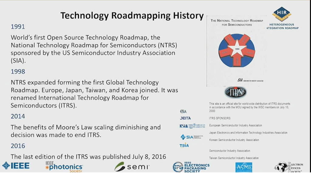
The ITRS committee regrouped in 2014 and started working on a new version of the roadmap that they felt would be better suited for the challenges facing the industry. Out of this effort, the Heterogeneous Integration Roadmap (HIR) evolved. The first version was published in 2019, The second version was highlighted at a SEMICON West 2021 tech talk on Heterogeneous Integration, where the 2021 road map was on the agenda.
Dr. Bill Bottoms, a co-chair of the HIR, shared a bit of the history and where they were going with the roadmap, highlighting the fact that the current roadmap is an electronic-systems- and market-applications-driven roadmap (Figure 2).
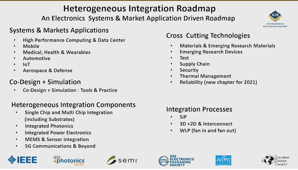
Figure 2: Systems and market-driven roadmap. (Source SEMI TechTalk Heterogeneous Integration)
The different sectors that the roadmap covers are fairly extensive. It spans from how to develop and evaluate critical materials needed at a faster pace than the industry has done historically, to what types of chips are needed to drive the different markets forward, and how those chips need to be packaged to successfully achieve the chips needed for specific applications. Along with that, we need to do this at a rapid pace to keep up with the projected growth rates for the industry.
Dr. Bottoms closed with the slide in Figure 3, which was presented by Dr. Gordon Keeler of DARPA at the Annual Conference for the Heterogenous Integration Roadmap in February of 2021. The slide points out the progress made over history with chips technology moving from geometric scaling to back-end-of-the-line (BEOL) scaling, 3D devices with FinFETS, and finally to heterogeneous integration. The slide also points out the distinct integration drivers; the slowing and added expense of following Moore’s law; and how using a 3D modular packaging strategy would enable low volume users to access cutting-edge technology at a lower cost.
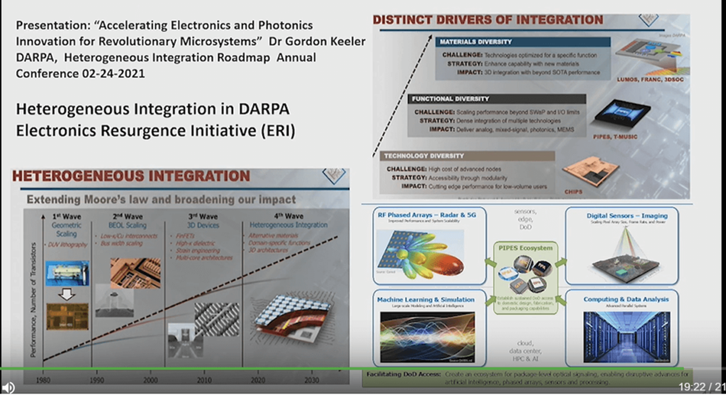
There is also functional diversity, of which heterogeneous integration will be a key enabler. The new packaging techniques and standards that will be developed will drive new systems that will combine MEM’s, photonics, analog, and other technologies, with logic and memory on the same package thus creating unique application-specific systems for industry use.
Dr. Bottoms did not go into great detail on specifications, or the actual roadmap itself. This was a bit disappointing due to my history of attending most roadmap releases over the history of the ITRS. The roadmap is supposed to have finished peer review by the end of 2021 so it should be available to download, and you’ll be able to peruse the roadmap and specifications soon.
CHIPS Act Update
Dr. Frank Gayle, Deputy Director, Advanced Manufacturing National Program Office Led off the seminar with a talk on the Department of Commerce and the NIST CHIPS act program overview. The fact that NIST is so heavily involved was a bit of a surprise to me as I have been used to DARPA driving programs that advance chip technology.
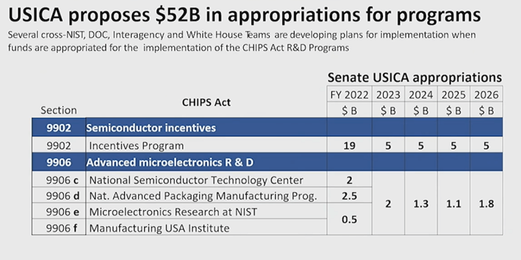
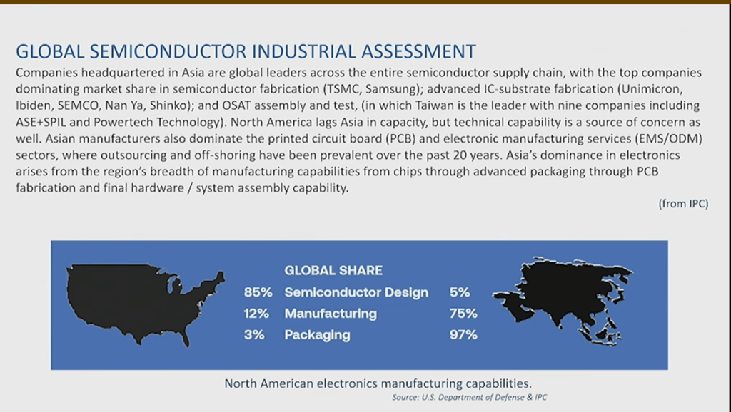
Dr. Gayle first broke down the proposed spending status for the CHIPS act. He commented that for advanced packaging in 2022 there is a proposed $5 billion spending budget. Figure 4 breaks the total spending down. As the bill has yet to pass, there is still some discussion on exactly how spending will be broken down, and NIST is taking input on how to best allocate the money. Dr. Gayle then went on to discuss a bit on how the industry is broken down on a worldwide basis, which in part helped to decide how the amounts of money above are to be broken down. Figure 5 shows the US Global share, which helped drive the decision to focus on advanced manufacturing and advanced packaging.

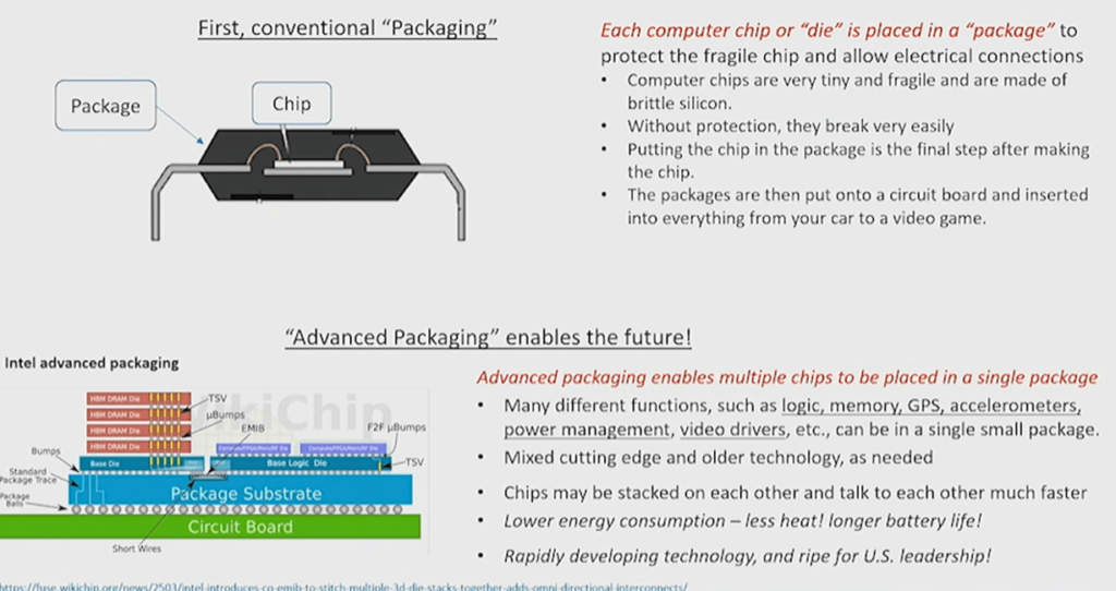
Dr. Gayle then discussed some of the challenges the NIST and other technical government departments have had in explaining semiconductor chips and packaging to government officials. With the shortages in chips for everyday items and automobiles, one would think that our educated elected officials would be able to distinguish a semiconductor chip from a potato chip or a corn chip. And that perhaps someone on their staff would have enough technical wherewithal to help them understand packaging and advanced packaging, but unfortunately, that is not the case and from Dr. Gayle’s comments, it appears a great deal of rudimentary education regarding semiconductors is needed (Figure 6).
I always smile when the department of commerce or our elected officials discuss onshoring the semiconductor business and repairing the supply chain. Only one of the top 20 outsourced semiconductor assembly and test (OSAT) packaging facilities and one of the top 15 substrate manufacturers are located in the United States. This will make onshoring difficult in the near term, and why many in the semiconductor industry are hopeful that this $50 billion is just the first in many cash infusions to help reestablish chip manufacturing in the United States.
Dr. Gayle commented that in most discussions surrounding packaging, it is agreed that conventional packaging will not be brought back to the US, but the opportunity is ripe for the US to gain a significant foothold in advanced packaging, especially since Intel is one of the leaders in that space and has committed to an advanced packaging facility in New Mexico. However, where does this leave the supply chain, especially those 200 mm power management devices, and microcontrollers that are creating a significant pinch point in the manufacturing supply chain? For the time being, they will still be packaged overseas, so supply chain management and inventories will need to be managed carefully for some time to come.
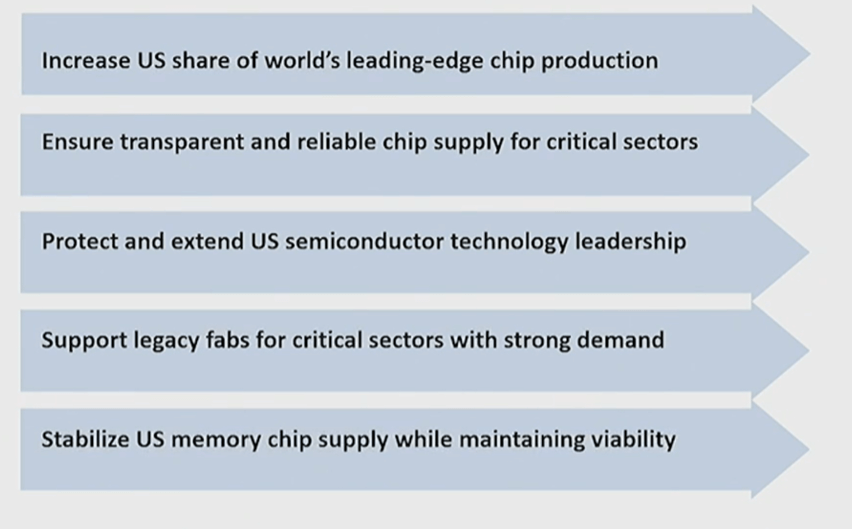
The high-level goals for the Incentive Program are focused on technical leadership, a reliable chip supply, increasing the production of leading-edge chips, and figuring out how to help legacy fabs with demand. Intel and Micron, already have world-leading development in their US facilities and can manufacture chips in the US. Adding capacity, as Intel has started to do, will continue to ensure leading-edge logic is produced in the United States. The program will need to incentivize Micron to build new fabs stateside instead of in Taiwan, or Singapore, where a considerable amount of memory packaging and final assembly of electronic systems takes place.
Another question is how do you onshore some of the leading-edge fabless companies such as Nvidia, Qualcomm, Xilinx, and AMD? Since in many cases Intel is a direct competitor, they won’t choose Intel as a foundry. Global Foundries can build some of these chips, but not at the leading edge, which means you need to incentivize TSMC and Samsung to build more leading-edge capacity in the United States for logic chips, as well as the advanced packaging needed so these chips don’t need to make a trip overseas before they are placed into inventory in the United States. To accomplish this, it will take considerably more than the $50 billion dollars potentially allocated.
So, from the presentation by Dr. Gayle, the good news is that there will be a great deal of focus on R&D in the US to maintain leadership in semiconductor manufacturing, manufacturing to ensure a reliable chip supply, and advanced packaging to assist in maintaining that advanced chip supply. The real question remains, will it get through Congress, and then will the local communities get on board helping the industry build facilities to ensure an onshore supply chain that is as economical as the one the industry has built over the past 30+ years when offshoring first began?


