

For 5G smartphones and other millimeter-wave (mmWave) applications, antenna integration, either through antenna-in-package (AiP) or antenna-on-package (AoP) technologies, simplifies the challenges associated with designing products that operate at these high frequencies. A variety of AiP/AoP design methodologies provide the required form, fit, and function for these applications and can include more than one antenna or an antenna array. Today’s AiP/AoP technologies can be implemented through standard as well as custom system-in-package (SiP) modules to achieve a complete radio frequency (RF) front-end (RFFE) subsystem.
Projected Growth for 5G, mmWave and RFFE Modules
In mmWave applications, signal loss becomes critical and the design challenges increase in complexity. In addition to emerging 5G smartphones, other applications that operate at very high frequencies and demand a small size include wearables, small cells, security cameras, radar units in autonomous vehicles, and numerous Internet of Things (IoT) wireless nodes. By 2023 over 1 billion mmWave units will be produced annually according to Gartner market research. With AiP technology, the antenna is no longer a separate component within the wireless device but is integrated in a SiP with RF switches, filters, and amplifiers. According to the consulting firm Yole Développement, the total RFFE module SiP market is projected to reach U.S. $5.3 billion by 2023, representing an 11.3% compound annual growth rate (CAGR).
AiP/AoP at Amkor
Instead of separate RF system on chip (SoC), baseband (BB) SoC, surface mount technology (SMT) matching circuits, and a discrete antenna, today’s fully integrated RF front-end module is completely achieved with AiP technology in SiP. In addition to a reduced size required for handheld and other small mmWave devices, AiP/AoP provides improved signal integrity with reduced signal attenuation and addresses the range and propagation challenges that occur at higher frequencies. As a leading outsourced semiconductor assembly and test (OSAT) supplier, Amkor has pioneered the packaging technologies required for RFEE subsystems (Figure 1).
Implementing AiP/AoP Technologies
Depending on the frequency range, different platforms are used for both the antenna and the IC package. In addition to AiP, the integrated antenna can be mounted on the package (AoP), or on a substrate (AoS), or in a SiP, mmWave antenna module and the AiP approach itself can vary from package to package. For applications below 6 GHz, a flip-chip ball grid array (FCBGA) or double-sided ball grid array (DSBGA) are two possibilities. For applications in the 28 GHz to 39 GHz range, the antenna could be a SiP module antenna or a flip-chip chip-scale package (fcCSP) with package-on-package (PoP) antenna. Applications in the 60 to 77 GHz range benefit from a wafer level or low-density fan-out (LDFO) package to the most advanced high-density fan-out (HDFO) packaging.
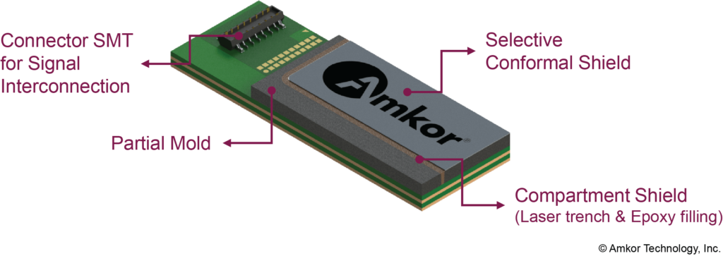
RF shielding techniques include dual-side mold, conformal shield, compartment shield using laser trench and paste filling technology, partial molding, selective conformal shielding, and hybrid SiP designs. These techniques implement a variety of materials to conductive lids as well as cored, coreless, and low coefficient of thermal expansion (CTE) and conformal shielding materials
Packaging technologies for AiP/AoP include:
- Body sizes up to 23.0 mm x 6.0 mm with several smaller options
- Up to 14 substrate layers
- Thin-film redistribution layer (RDL) and dielectrics for 77 GHz and higher applications
With Amkor AiP/AoP technologies, system designers get:
- A smaller footprint-phased antenna array design to minimize space
- Reduced signal attenuation for mmWave products
- Lower power consumption
- Improved range for devices
- A design proven and qualified by the supplier
In fact, Amkor’s AiP/AoP packaging technologies have achieved over 60 GHz operation.
Design Services & Design/Production Capabilities for AiP/AoP
For AiP/AoP technologies, Amkor has developed an extensive toolset to maximize circuit density and address the sophisticated packaging formats required for high-volume production of 5G and any mmWave design. In addition to an advanced multi-die integration toolbox and RF SiP design and simulation know-how, other capabilities include:

- Extensive fcCSP, WLCSP, LDFO and HDFO portfolios for multi-die designs
- An established and reliable supply chain
- Global assembly scale and system test investments
- RD design & measurement lab
Initiating an AiP/AoP Design
Amkor offers many options to incorporate AiP/AoP in a variety of packages or SiP and the high-volume production capacity to support the design of the next generation mmWave products. To integrate Amkor’s market-leading 5G and mmWave packaging technology in a next-generation application, system designers simply need to contact Amkor and discuss their system requirements.
About the Authors

Vik Chaudhry, Sr. Director, Product Marketing and Business Development Advanced Products, Amkor Technology, Inc. joined Amkor in 2014 as Sr. Director of Product Marketing and Business Development for Advanced Products BU. Prior to joining Amkor, Vik was Sr. Marketing Manager for Networking and Communication timing products at IDT. Prior to IDT, Vik held engineering and marketing management roles at White Electronics (MicroSemi), TDK Semiconductors, and Motorola SPS. Vik has also authored several technical papers. He holds a B.S. in Electrical Engineering from National Institute of Technology, Bhopal, India, and a Master’s Degree in Electrical Engineering and an MBA from Arizona State University.

Curtis Zwenger, VP, Adv. Package & Technology Integration, Amkor Technology, Inc. joined Amkor in 1999 and has held leadership roles in developing Amkor’s Fine Pitch Copper Pillar, Through Mold Via and MEMS packaging technologies. He is currently responsible for the development and commercialization of Amkor’s Advanced Wafer Level Fan-Out package technologies, including High-Density Fan-Out and SWIFT® technology. Curtis is Past General Chair of the International Wafer-Level Packaging Conference 2016-2018 and the 2019 General Chair for the IMAPS Symposium on Microelectronics. He has authored numerous technical articles and papers and co-authored a chapter in the recently released book, “Advances in Embedded and Fan‐Out Wafer‐Level Packaging Technologies”. Curtis has been issued 21 US patents and holds a degree in mechanical engineering from Colorado State University and an MBA from the University of Phoenix.
© 2020, Amkor Technology, Inc. All rights reserved.
This article appears in the 3D InCites Yearbook. Download your copy here.


Comments are closed.