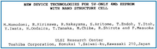
Part 3 of the series, The Triumph of Quantum Mechanics at the Heart of Solid-State Data Storage, continues with the invention of NAND flash memory. The above image is of the first comprehensive paper reporting the NAND Flash invention where Fowler-Nordheim tunneling is used for program and erase of the memory. [1]
After the fundamental studies in the late 1960’s Quantum Mechanical tunneling started to appear in silicon integrated circuit products as the program and erase mechanism.
Figure 18 shows excerpts from Eli Harari’s 1978 patent on the silicon electrically erasable nonvolatile semiconductor memory where Fowler-Nordheim tunneling through a thin tunnel oxide to and from a MOSFET floating gate is used as the program and erase mechanism. This was the practical implementation of D. Kahng and S.M. Sze’s floating gate concept shown in Figure 12 (see part 2).
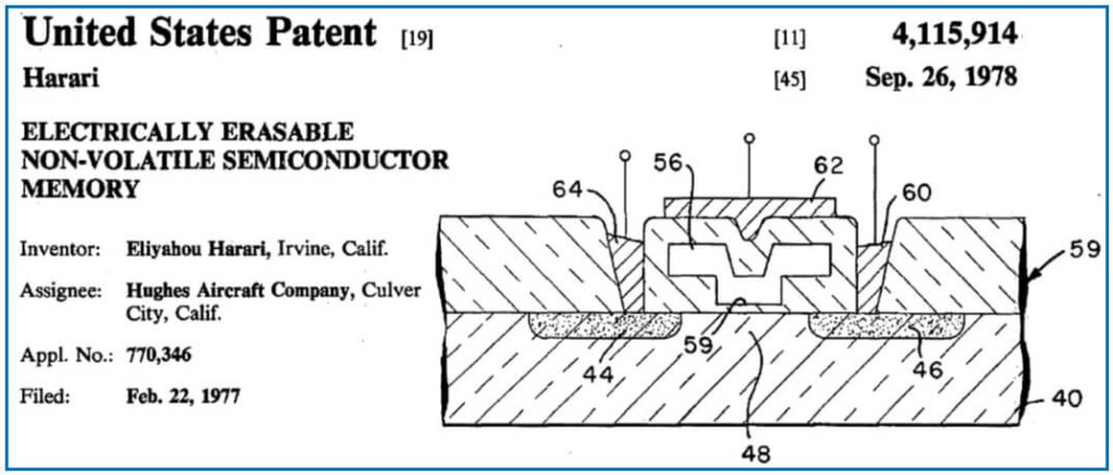
Figure 18 shows the fundamental elements common to all silicon nonvolatile memories relying on charge storage, namely:
- A MOSFET in which the threshold voltage depends on the charge stored in a reservoir (56) located between the MOSFET gate (62) and the silicon channel (48).
- A mechanism to change the amount of charge stored in the reservoir and therefore the MOSFET threshold voltage. In Figure 18, this mechanism is Fowler-Nordheim tunneling.
- The design of the MOSFET memory such that the stored charge remains in the reservoir without external power applied.
The use of the floating gate concept started to become the dominant approach for charge storage in silicon nonvolatile memory products in the late 1970’s and early 1980’s. Nevertheless, charge storage in a silicon nitride layer remained as the preferred method among several companies. We shall see shortly how silicon nitride is now making its return in the most advanced nonvolatile memories.
More than 20 years after D. Kahng and S.M. Sze’s floating gate concept, the application of Fowler-Nordheim tunneling for both program and erase in a very area-efficient memory cell came in 1988 with the invention of NAND Flash.
NAND Flash has become the dominant approach for solid state data storage. Three reasons for this stand out:
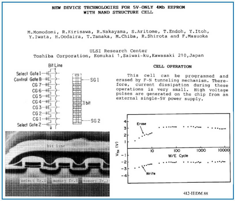
- NAND Flash is extremely area-efficient since area-sapping metal contacts are used sparingly. For example, in Figure 19, half a contact per string is used to connect to the bit line and half a contact per string to connect to the ground line.
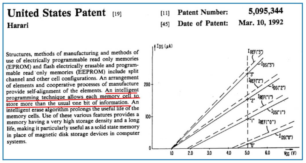
- Methods had been invented around the time of NAND’s introduction to store more than one electrical bit per cell by controlling the number of electrons that tunnel into the floating gate. This multi-state approach effectively increases the digital data density in the NAND chip. Figure 20 shows the introduction of this approach.
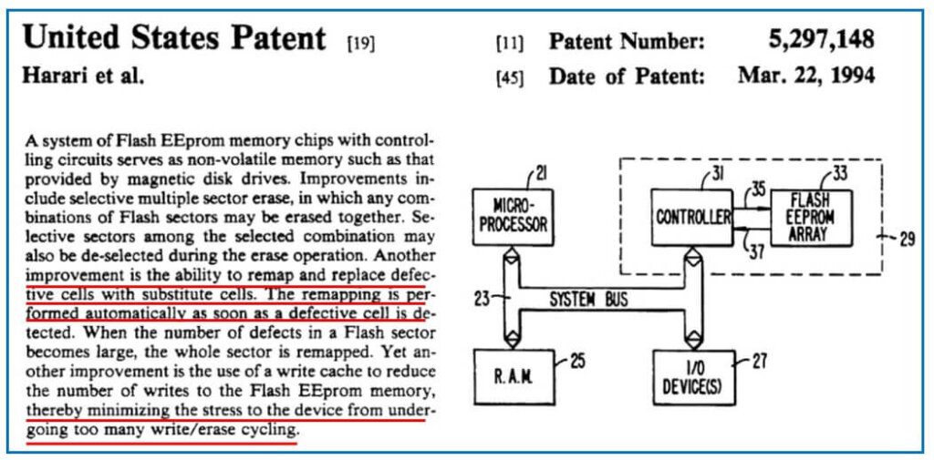
- Techniques at system level had been introduced soon after NAND introduction to control and monitor memory cell damage arising from Fowler-Nordheim tunneling program and erase. Figure 21 shows the first implementation of this. This became known as “System Flash”.
Between 1988 and 2016, the NAND Flash cell has been physically shrunk by more than 10000 times. With the multi-state ability to store three electrical data bits per cell, the effective cell area has been shrunk by more than 30000 times.
Figure 19 above showed a 4 Mbit (4 million bits) as the first NAND Flash chip. With tens of thousands of shrink factors over more than 25 years, the latest NAND Flash chips have capacities in the 200 Gbit (200 billion bits) range.

This enormous increase in memory storage capacity coupled with the ability of the silicon semiconductor industry to continuously drive down the costs per bit has resulted in the solid state data storage revolution.
Figures 22 and 23 show high-resolution transmission electron micrographs of two of the most advanced NAND Flash chips in the market today. Both are made using 16nm NAND Flash technologies. The fundamental structure of D. Kahng and S.M. Sze (Figure 12) and E. Harari (Figure 18) is evident with the floating gate buried into a MOSFET structure.
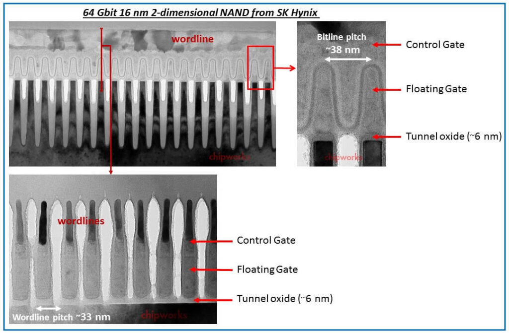
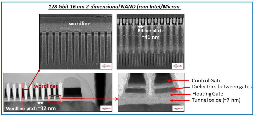
And between the floating gate and the silicon channel, we find the tunnel oxide, the link to the quantum mechanical tunneling discovered in the 1920s, applied to silicon memory devices in the 1960s, developed through the 1970s and 1980s that resulted in the invention of NAND Flash in the late 1980s and continuously shrunk ever since to reach the enormous data storage capabilities of today. ~ A. Walker
Read the whole series from the beginning.
References
- M. Momodomi et al., International Electron Devices Meeting 1988)