
Continuing our look out into the future, at the recent Hot Chips Conference, Dr. Phil Wong, VP of R&D at TSMC gave a presentation entitled “What Will the Next Node Offer Us?” where he discusses the use of chiplets, 3DICs, and a futuristic technology for the heterogeneous integration of memory and logic called N3XT, noting that this technology will be necessary after 3D in order to combine multiple layers of logic and memory with dense TSVs.
For a little deeper look at N3XT let’s examine a 2019 presentation by Subhasish Mitra, Prof. of Computer Science at Stanford on their N3XT work with MIT.
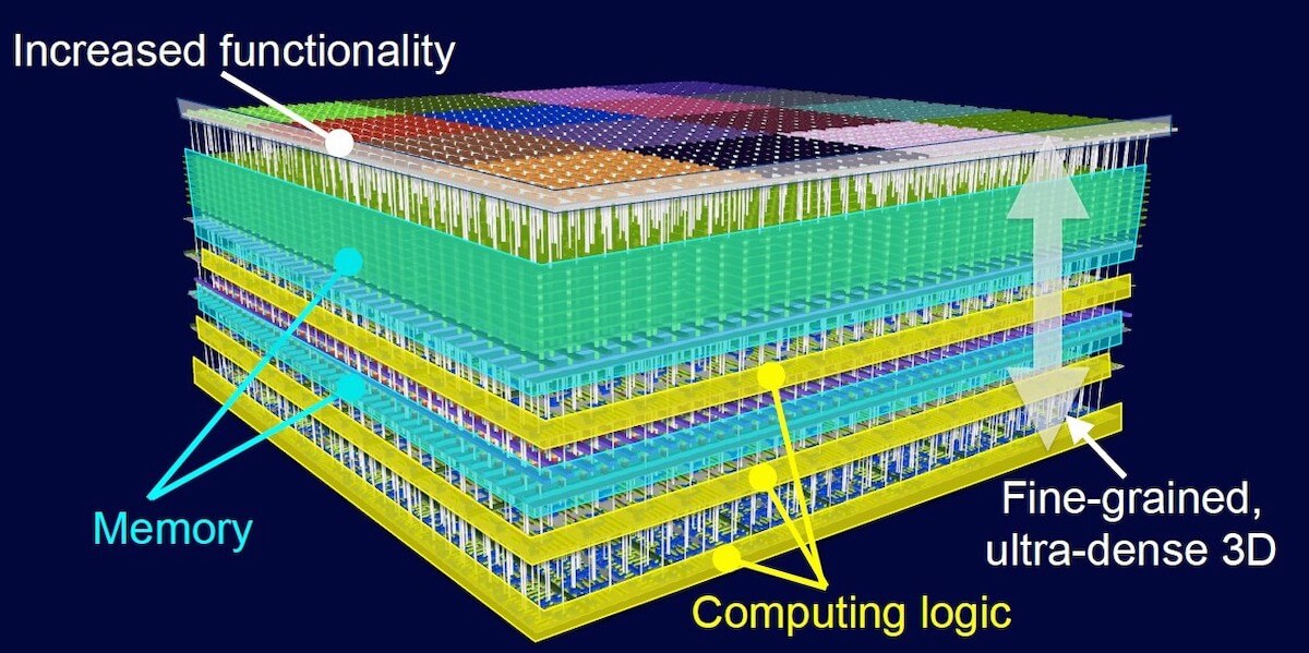
N3XT reportedly will improve the energy efficiency of abundant-data applications 1,000-fold by using new logic and memory technologies, 3D integration with fine-grained connectivity, and new architectures for computation immersed in memory. The 3D stack replaces silicon with carbon nanotubes and integrates resistive random-access memory (RRAM) cells. CNFETs are an emerging transistor technology that reportedly can scale beyond the limits of silicon MOSFETs and promise an order-of-magnitude improvement in energy-efficient computation.
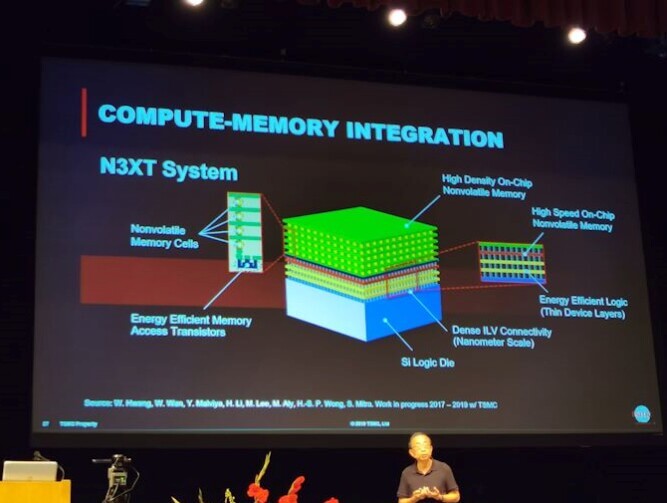
The researchers integrated more than 1 million RRAM cells and 2 million carbon-nanotube field-effect transistors in the chip, reportedly making it the most complex nanoelectronic system ever made with emerging nanotechnologies.
Instead of requiring separate components, the RRAM cells and carbon nanotubes are built vertically over one another, creating a dense new 3D computer architecture with interleaving layers of logic and memory (Figure 2).

It is reported that carbon nanotube circuits and RRAM memory can be fabricated at temperatures, below 200°C, whic means they can be built up in layers without harming the circuits beneath them. Such integration will require much denser TSVs as shown in figure 3.

On the top layer of the chip they placed over 1MM carbon nanotube sensors to detect and identify ambient gases. The chip was able to measure each of the sensors in parallel, and then write directly into its memory. This work was funded by the Defense Advanced Research Projects Agency, the National Science Foundation, Semiconductor Research Corporation,
The Chiplet Story Continues
In IFTLE 423 we discussed TSMC / ARM module for HPC derived from chiplets and an interposer. We are now getting further information on this system.
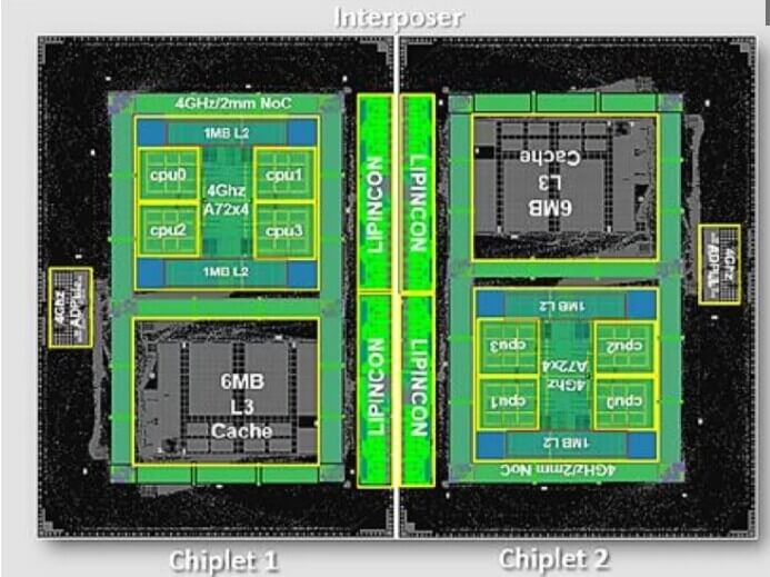
The system that TSMC and ARM presented consists of two 7nm FinFET chiplets with four Cortex-A72 cores, connected via a “bi-directional interconnect mesh bus operating at 4GHz. The chiplet has 2MB of L2 and 6MB of L3 cache. The system taped out in December 2018 and was produced in April 2019 (which gives a rough indication of 7nm’s cycle time).
The interconnect is built using TSMC CoWoS interposer technology and TSMC’s LIPINCON (Low-voltage-In-Package-INterCONnect ) architecture. Recall from IFTLE 423 that this is TSMCs alternative to Intel’s AIB and MDIO chiplet interconnect. LIPINCON operates at 0.3V and has a bandwidth of 8Gb/s per pin and 320GB/s total bandwidth.
This module serves as TSMC’s proof-of-concept for LIPINCON interconnect, which TSMC indicates could appear in commercial products next year.
For all the Latest on Advanced Packaging stay linked to IFTLE…………………………….


