
It was exactly a year ago that GLOBALFOUNDRIES’ announced that they would no longer be competing in the node scaling race. I wrote that up in IFTLE 395, the last IFTLE post written for Solid State Technology whose parent, Extension Media was headed for bankruptcy. I cannot give you the link because it is no longer there. If you sense some bitterness in my writing, there is, because I can no longer link you to IFTLE 395 or any other IFTLE …poof……one of the major problems of the internet.
At the time, GLOBALFOUNDRIES canceled 7nm work and all pathfinding and research operations for 5nm and 3nm nodes.
3D Chip Stacks Offer an Alternative to Node Scaling
It now appears that they have concluded that 3DIC (AKA 3D chip stacks), an alternative to costly node shrinking, may help GLOBALFOUNDRIES maintain a market presence. GLOBALFOUNDRIES has just announced that it has taped-out a 3D test chip for “..high core artificial intelligence (AI) designs, cloud computing, and mobile SoCs”.
GLOBALFOUNDRIES has been looking at 3D chip stacks and 2.5D for a while. In 2012 GLOBALFOUNDRIES announced that it had begun the installation of special production tools to create 3D through silicon via (3D TSV devices processed on its 20nm technology platform, at its Fab 8 campus in N.Y.
The new chip was reportedly fabricated using GLOBALFOUNDRIES’s 12nm FinFET process and features ARM’s mesh interconnect technology in 3D that allows data to take a more direct path to other cores, minimizing latency while increasing data transfer rates as demanded by data centers, edge computing, and high-end consumer applications.
Moreover, the companies report that they have validated a 3D design-for-test (DFT) methodology, using GLOBALFOUNDRIES’s hybrid wafer-to-wafer bonding that can enable up to 1 million 3D connections per mm2.
John Pellerin of GLOBALFOUNDRIES reports that “In the era of big data and cognitive computing, advanced packaging is playing a much larger role than it has in the past. The use of AI and the need for power-efficient, high-throughput interconnect is driving the growth of accelerators through advanced packaging.” He also says that GLOBALFOUNDRIES’s 3D face-to-face (F2F) packaging (bonding) solution “…not only provides designers a path to heterogeneous logic and logic/memory integration but can be manufactured using an optimum production node that enables lower latency, higher bandwidth, and smaller feature sizes”.
IFTLE cannot find any released pictures or further technical details yet, but I’m sure something will be coming soon.
TSMC Lead the Way at 7nm
IFTLE assumes this GLOBALFOUNDRIES 3D work is meant to compete with technology at lower nodes such as the recent 2.5D work of TSMC at 7nm. In June at the 2019 VLSI Symposium in Kyoto, TSMC demonstrated a 7nm ARM-based chiplet design with mesh interconnect for HPC based on their 2.5D chip-on-wafer-on-substrate (CoWoS).
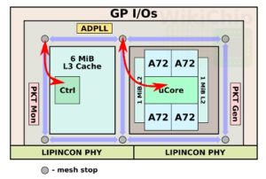
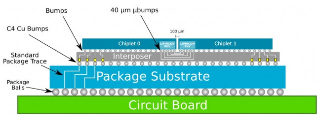
Each TSMC chiplet is manufactured on TSMC 7nm with 15 metal layers. The die is 4.4 mm by 6.2 mm and contains four ARM Cortex-A72 cores (Figure 2). The die similarly includes mesh interconnect. The mesh interconnect is 1968-bit wide and are routed in M12 and M13 using interleaved wires with opposite direction signals to minimize coupling. All in all, the on-die mesh interconnect can operate up to 5 GHz (1.2 V). The interconnects can reach a frequency of 4 GHz at 0.76 V.
TSMC uses their CoWoS 2.5D packaging technology for the two identical chiplets which are mounted on top of it. 40um micro bumps enable dense and low power wires between the chiplets which are separated by only 100 µm.
For all the latest in Advanced Packaging stay linked to IFTLE…………………………………

