

It’s almost ironic. As CMOS scaling (aka: Moore’s Law) has slowed due to the increased complexity and cost of achieving smaller nodes, the focus has shifted to advanced packaging and heterogeneous integration to meet demands for microelectronics devices targeting the internet of things (IoT) market. These devices perform a variety of functions (sensing, processing, remembering, transmitting) in smaller spaces, using less power. To do this, advanced packages are designed with finer features, need higher density metal patterns, and multi-layer redistribution layers (RDLs).
And suddenly, advanced packages have become as complicated and valuable as the chips they are designed to integrate and protect. With higher value comes a higher concern for improved reliability and yields. As a result, foundries who have expanded their advanced wafer level packaging (AWLP) capabilities and outsourced assembly and test service (OSATS) providers are demanding more sensitive, inspection, metrology and data analysis—and more accurate identification of bad parts. Not quite the level of inspection used in the front end… but something fairly close.
I recently interviewed KLA Tencor’s Lena Nicolaides, Stephen Hiebert, and Pieter Vandewalle to learn about the company’s recent developments in metrology and inspection for advanced wafer level packaging and final package inspection, designed to address some defect types that have become more prevalent as advanced packages have become more delicate.
The Role of defect inspection
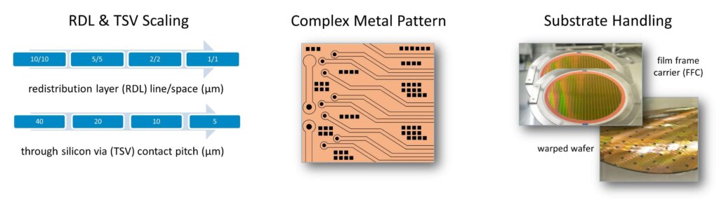
Defect challenges for wafer level packaging include smaller killer defects due to feature sizes, nuisance defects due to complex, dense metal patterns, and high warp wafers and film frame carriers for accommodating different thickness wafers, as well as reconstituted wafers (Figure 1).
As Hiebert explained it, defect inspection is particularly important during wafer level packaging processes for quality control, process control, and engineering analysis. It helps identify excursions both while they can still be reworked and repaired, and again to identify defects that can’t be fixed but can cause more problems if they are allowed to continue through the processes. Through in-line monitoring, causes of defects can be characterized and the processes tweaked, with the goal of improving final yields.
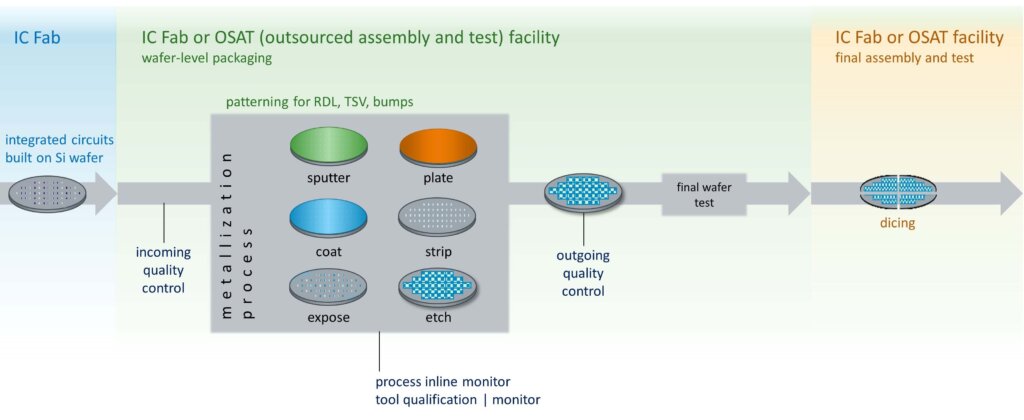
Additionally, increased package complexity calls for additional inspection steps. “In a chips-first approach to fan-out wafer level packaging (FOWLP), there are typically three layers of RDL and 2-5µm line/space requirements,” said Hiebert. “this calls for up to 16 inline inspection steps.” These come at different points throughout the process, the most critical are after the develop step during lithography, and again after the etch process in base-metal etch.
Defect inspection plays a similar role in test and assembly, although the focus is on outgoing quality control, and not necessarily process control. What’s different for the newest wafer level packages, explained Vandewalle, is that previously wafer level packages did not go through the same test and inspection as legacy packages like leadframe and substrate-based packages. But now, high-end node chips manufactured with low-k materials which are more brittle and subject to defects (especially after dicing) require advanced inspection, especially to capture chipping, hairline cracks, and laser groove cracks.
“One reason we decided to pursue this market was that there is no good technology outside of an R&D environment designed to capture these types of new defects, such as sidewall cracks,” he explained. “So, we invested in new IR-based technology for the production environment.”
KLA-Tencor’s solutions
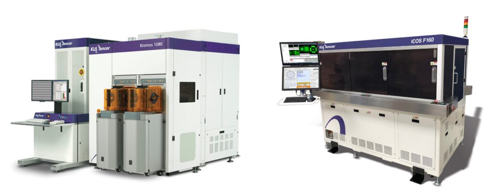
More than three years in development, KLA-Tencor just launched two new systems, the Kronos™ 1080 and the ICOS™ F160, targeting some specific needs of advanced wafer level, 2.5D and 3D integrated packages. (Figure 2)
Building on lessons learned with their front-end systems, as well as their existing packaging offerings, CIRCL™-AP, and the ICOS™ line, the company worked in close partnership with its existing customers to identify the gaps in current inspection strategies and develop these systems, explained Nicolaides.
“Our customers who lead in scaling technology came to KLA-Tencor looking for sensitivity beyond what the back-end players could traditionally achieve,” she explained. “We designed these systems’ architecture and algorithms for a superior cost of ownership, ability to find defects while offering increased throughput and overall yield improvement.”

Kronos 1080
The Kronos 1080 system is designed to inspect advanced wafer-level packaging process steps, providing information on the full range of defect types for inline process control through multi-mode optics and sensors and advanced defect detection algorithms. Its proprietary FlexPoint™ technology focuses on the inspection system on key areas within the die where defects would have the highest impact (Figure 3).
ICOS F160
Vandewalle described the challenges in final package inspection that the ICOS F160 is designed to address, namely low-k cracks on sidewall and laser grooves that are difficult to detect. The system’s purpose is to be used in high-volume manufacturing to separate out the bad parts and keep the good.
In designing the ICOS F160, Vandewalle said the focus was finding a solution to address dicing cracks caused by an aggressive dicing practice. Existing approaches relied on either optical or open/short tests, but none was good enough to capture critical defects. He said that as a result, the packages fail in the end-use device, and mobile and wearable companies are suffering from the slip-through.
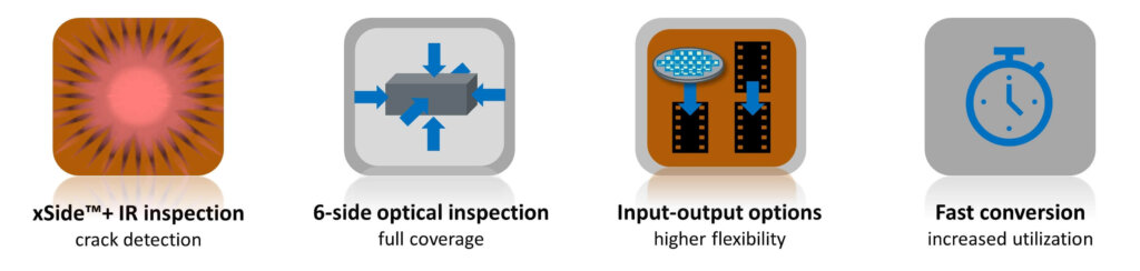
The ICOS F160 features IR inspection, which provides robust detection of invisible killer crack defects for fan-in wafer-level packages, memory and bare die. In combination with 6-side optical inspection with pre-and post-placement inspection, the ICOS F160 enables high die sorting accuracy. Additionally, the system’s flexibility allows it to support a variety of workflows, including wafer-to-tape and tape-to-tape. Lastly, fast conversions, automatic calibration, and precision die pickup addresses the needs of high-volume manufacturing.
Where the action is
While CMOS scaling may continue, advanced WLP is clearly where the action is, driven by the IoT explosion. Because advanced packaging technologies are so much more varied than front-end processes, the greatest challenge for KLA Tencor was developing systems next-generation inspection systems that are both flexible and high-performing.
“There’s always a trade-off. The more flexible you make something, the more challenging it is to achieve optimized performance,” said Nicolaides. “After analyzing the requirements of the diverse package designs, we focused on defect sensitivity and inflection points to leverage our optical expertise.”
The result of that focus has been realized in the addition of these two systems to their product portfolio.
Learn more about Kronos 1080 and ICOS F160 here.


