
While critical to the processes, molding and encapsulation materials used in both fan-in and fan-out wafer-level packages (FI WLP/FO WLP) can lead to high wafer warpage after molding, which may ultimately lead to downstream wafer handling issues. Additionally, many of these materials contain certain anhydrides that are banned under the guidelines of the EU REACH legislation, identifying them as substances of very high concern (SVHCs) that could potentially be a supply chain risk. This Henkel white paper discusses a low-warpage, high UPH, REACH-compliant liquid compression molding material that overcomes high wafer warpage and enables higher reliability FO WLP and FI WLP devices.
Fan-In Wafer-Level Packaging (FI WLP) and Fan-Out Wafer-Level Packaging (FO WLP) are two approaches that are showing promising cost efficiency and performance benefits as indicated by their market growth. According to market analyst, Yole Development, the CAGR from 2016 – 2022 for FO WLP is 31%, while FI WLP is projected to see 8% growth in the same period. For applications like data processors, mobile devices, and automotive industrial systems, the advancement of these technologies is good news.
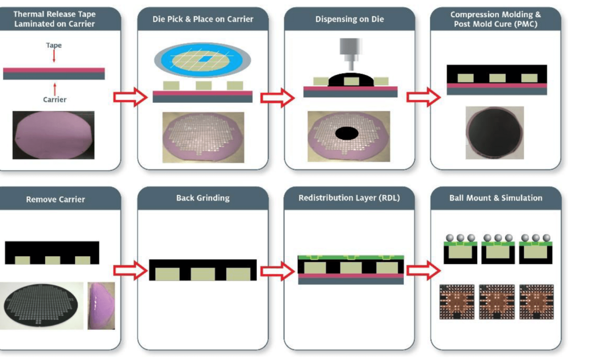
FO WLP is an extension of standard wafer-level packaging (WLP), but one that enables more I/O connections without having to increase the die size, allowing for a smaller package footprint with improved thermal and electrical performance. The process flow for FO WLP as compared to traditional WLP, where integrated circuits are packaged while they are still part of the wafer, is different. In FO WLP processing, the wafer is diced first and the dies are then placed onto a carrier, which is then compression molded. A redistribution layer is made on top of the entire molded area, following which solder balls are mounted onto the top.
Alternatively, FI WLP is a technology in which an integrated circuit is packaged at the wafer level as opposed to the fan-out approach of assembling various dies into a package after wafer dicing. The FI WLP approach is suitable for packaging dies with low input-output (I/O) counts. With this technique, a redistribution layer is used to connect copper pillars or bumps/balls on top of the die surface. Trenches are cut in between the individual dies, then filled with a molding material to offer device protection prior to grinding and dicing into single units. Liquid compression molding (LCM) material — is critical for handling to enable subsequent process steps and also to protect against warpage.


Comments are closed.