


NCP and NCF Property Optimization Delivers High-Reliability Results
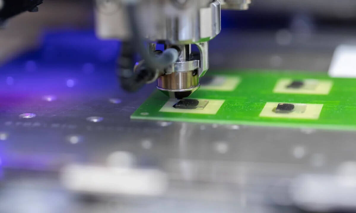
Semiconductor package sizes are getting smaller and bump pitches narrower while the number of input/output (I/O) continues to increase. The traditional flip chip process, which assembles the chip with copper (Cu) pillar interconnects to the substrate using a mass reflow technique, faces several hurdles as package dimensions become more challenging. Good alignment and reliable joint interconnections are becoming difficult to achieve, particularly when the bump pitch is less than 100 µm. Pre-applied underfills like non-conductive paste (NCP), applied directly on the substrate, and non-conductive film (NCF), which is pre-applied on the wafer, enable the thermocompression bonding (TCB) process which can help overcome these challenges, as long as the process is optimized.
During the NCP TCB process, void issues are common and several factors (e.g. dispensing volume and pattern, bonding parameters, and material properties) may contribute to void formation. A study was conducted to evaluate different dispensing patterns to better understand this issue and identify patterns that may help reduce voiding. The effect of bond speed on void performance was also analyzed. Within the NCF TCB process, the impact of bond parameters on void performance was evaluated, with a particular focus on the influence of bond force, contact temperature, and ramp rate on bond optimization.
This white paper from Henkel presents a summary of the findings and reveals the optimum conditions for improving reliability when using NCP and NCF materials in a TCB process.
Authors: Promod Chowdry, Rose Guino, Kail Shim, Kevin Lindsey, Jie Bai, Gina Hoang, and Ramachandran Trichur, Henkel Corporation


