The semiconductor packaging industry continues to advance, with new designs adding more layers, finer features, and more I/O channels to achieve faster connections, higher bandwidth, and lower power consumption. As packaging technologies have evolved, manufacturers have adapted old processes and adopted new processes to connect chips to each other and to the outside world. Often these new processes use front-end-like tools and techniques to perform back-end tasks, blurring the traditionally sharp distinction between the two ends. This area of overlap has been called the middle-end and its growing importance has created an increasing need for specialized, high-precision measurement and inspection capabilities to detect defects and improve process control.
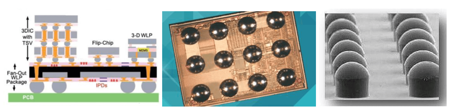
The latest advanced packaging techniques seek to integrate more power and functionality in a single package that uses less space and has more numerous, shorter, faster connection paths. Most use some form of vertical integration, stacking chips on top of each other or on specially designed substrates (Figure 1).
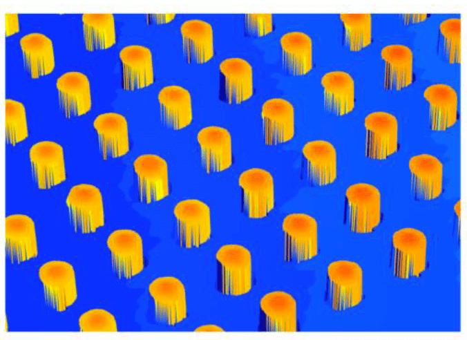
functionality in less space. Many advanced packaging processes use solder bumps and pillars for vertical connections. (Source: Yole Developpment, Amkor)
Vertical connections are frequently made using bumps or pillars that extend above the surface of the chip. Because these processes use known good die, the cost of failure is high. The cost of failure can be even greater when the health and safety of the user is at risk, as in automotive applications for assisted driving or self-driving cars. Fast accurate inspection and measurement of these and other similar structures is a critical requirement for improving yields and ensuring reliability.
A multiple reflection suppression sensor (MRS) that uses phase shift profilometry (PSP) may be the answer. PSP uses structured light to measure three-dimensional (3D) objects. The MRS sensor projects a fringe pattern on the object and looks for shifts in the pattern that appear when surfaces at different heights are viewed from an angle to the projection direction. To learn more about this technology, download the free white paper, NanoResolution MRS Sensor Delivers Fast, Precise 3D Inspection and Measurement for Advanced Semiconductor Packaging Applications, By Tim Skunes.