

Like many other industry conferences, the Electronic Design Process Symposium (EDPS 2020) had to go virtual. Not only did it keep our audience safe but allowed us to attract almost 200 registrants worldwide. Thanks to sponsorships from – ANSYS, Cadence, CEDA, Intel, Mentor – A Siemens Business, and Synopsys – attending EDPS 2020 live was free. The only disadvantage was the loss of high-value face-to-face networking with semiconductor industry visionaries. This year’s “networking” is limited to follow-up email and phone calls.
Full disclosure: In 2012, Gary Smith encouraged me to join the EDPS organizing committee to add attention to manufacturing-related topics.
The EDPS 2020 Speaker Line-Up
Intel’s Raymond Rodriguez, this year’s General Chair, summarized the long history: The first EDPS was held in Breckenridge, Colorado, in 1990, then EDPS moved to Monterey, California, to get closer to Silicon Valley. Its focus was on electronic design automation (EDA) design methodology. In 2017, SEMI invited EDPS to its headquarters in Milpitas/Silicon Valley, where we (hopefully) will hold EDPS 2021.
To serve many different time zones live, we webcast on Wednesday morning, Sept 30, presentations from:
- TSMC: Advanced IC Packaging
- HP Labs: Photonics
- ANSYS Granta: Materials Characterization and Modeling
- Facebook: Taming Carbon Pollution
- Intel: Data Center Security
- IBM: Quantum Computing Hardware.
On Thursday afternoon we webcast presentations from
- University of Chicago: Design of Superconductor Circuits for Quantum Computing
- Intel: Interconnect Scaling in Advanced IC Packages
- ANSYS: Leveraging Simulation-based Digital Twins in Manufacturing and Maintenance
- Amkor: Using Machine Learning (ML) to Optimize Semiconductor Test
- Stanford/Cerebras: ML on Massively Parallel Hardware.
The MP4 files of all ~ 20 minutes presentations and the Q&A sessions have been recorded and are posted, together with the slides, on the EDPS website for on-demand viewing.
The Impact of Materials, Architectures, and Test
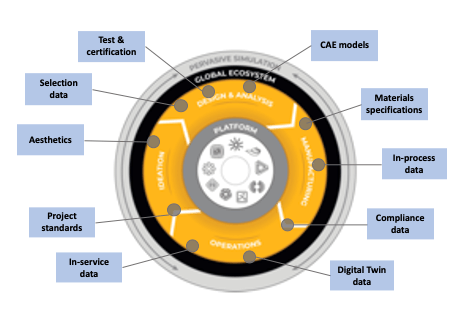
Andrew Miller is Director of Data Products and Collaborative R&D at Ansys Granta in the UK. He explained the importance of accurate materials characterization and modeling data as inputs for a broad range of simulators. These data enable designers to assess material cost, design margins, timing, reliability, power consumption, and many other characteristics of a complete product through its entire life cycle. How the deployed materials behave oversupply voltage, temperature, humidity, physical stress, vibration, shocks, and many other parameters are essential for the design of cost-effective and reliable products. Miller also explained the Granta MI data management system – see Figure 1. It gives users quick and easy access to the vast amount of accurate materials data the ANSYS Granta team has captured and multi-physics simulators require.
Ravi V. Mahajan is an Intel Fellow responsible for Assembly and Packaging Technology Pathfinding for future silicon nodes. He holds the original patents for silicon bridges that became the foundation for Intel’s Embedded Interconnect Bridge (EMIB) technology. In this presentation, Mahajan explained first the ongoing multi-die Heterogeneous Integration Roadmap (HIR) and why it replaced the single die SoC-centric ITRS efforts in 2017. Then he showed why the continuation of interconnect scaling in advanced packaging architectures is important. Tighter pitches between chiplets enable higher bandwidths and lower interconnect power dissipation – see Figure 2.

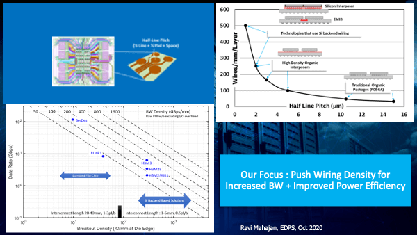
Majahan pointed out that Intel has a lot of experience with design and manufacturing topics for die-to-die interconnects up to 10 mm long, and referred to an ECTC 2019 paper titled: “Electrical Performance Limits of Fine Pitch Interconnects for Heterogeneous Integration” for more in-depth information. Intel describes in this paper the impact of dielectric constant, wire length/material/cross-section, horizontal/vertical design rules and routing density, signaling speed, and receiver sensitivity.
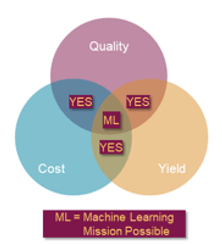
Gerard John is Senior Director of Advanced Engineering Services (Global) at Amkor Technology, Inc. and has lots of experience with multi-die IC test and debug. He started his presentation, titled “Using Machine Learning to Optimize Semiconductor Test” with an explanation of ML basics, like supervised and unsupervised learning, classification, regression analysis, and clustering, then explained how ML techniques can be applied to a BGA’s opens-and-shorts test routine, that utilizes the ESD diodes to source/sink current during test. Even this simple example gave a good picture of how ML can reduce cost, improve yield, and product quality – see figure 3.
In the Q&A portion, Gerard confirmed that a test team’s EDA partner(s) play(s) important roles to make ML truly effective and efficient, e.g. develop tools that generate specific ML training routines in every circuit’s test program and place test steps that are likely to fail early in the test program – to eject a bad part early, before it would consume more valuable tester time.
Personal Comments
For many years, the late Gary Smith, in his roles at DataQuest, Gartner, and Gary Smith EDA, encouraged our industry to see ourselves as solvers of system-level problems, not component experts. Every one of this year’s presenters demonstrated that we finally are listening to him. We addressed system topics either directly or enablers towards it, like infrastructure, architecture, and ecosystem. Gary Smith would be glad to see this and tell us: “Better late than never!”
Last but not least, I would like to thank our sponsors, the professional organizers, and the excellent speakers to work together on this content-rich EDPS event. Check it out here!


