
In the early days of ASIC technology, only logic library elements and basic I/Os with up to 10s of transistors were available for customizing gate arrays and/or logic functions in standard cell chips. And then, “megacells” (a.k.a. Functional Blocks, Semiconductor IP Blocks), comprised of 100s, even 1000s, and more transistors became available and offered proven memories, processor cores, data converters, special I/Os and many other widely used functions for integration in IC designs. These megacells enjoyed rapid market acceptance, mainly because they boosted designers’ productivity, reduced risk of failure, and cut development as well as unit cost.
History Repeats Itself
While Moore’s Law has driven major progress in integrating many functions into small pieces of silicon (a.k.a. die, plural dice), IC packaging experts at IDMs, assembly houses (a.k.a. OSATs) and wafer foundries have developed technologies to integrate one or more of these delicate dice into an IC package, primarily to protect it/them against mechanical damage and avoid over-heating. Because advanced packaging technologies have made it technically easier and more cost-effective to combine multiple dice in a package, calls for repeating the success of ASIC megacells for advanced packaging became louder. Developers responded and the term “chiplet” was coined for a die that is ready for integration into a package and can interface with other chiplets in this package.
As a complete product, a chiplet includes not only the physical die but also models/electronic datasheets that describe – e.g. core functionality, physical dimensions, power dissipation, footprint, location of power/test/signal pins and I/O characteristics. These models/electronic datasheets enable EDA planning, design, and verification tools to integrate chiplets relative quickly into a suitable single-die or multi-die package, optimize power, unit cost, reliability, and ensure first-time success. High bandwidth memory (HBM) devices were the first chiplets offered; FPGA slices, SerDes I/Os, processor cores, hardware accelerators, and other functions followed. A chiplets can be proprietary – to differentiate an IC – or available from 3rd parties who specialize in widely used functions – e.g. HBMs and SerDes.
While EDA companies – for business reasons – typically wait for new technology to mature and standards to solidify, before supporting it to automate design steps, the rising market demand for chiplets has encouraged the EDA industry to dedicate time at DAC 2020 for addressing chiplets. Tutorial 10, titled Chiplet Integration: Tools, Methodologies, Requirements, Infrastructure covered in two-parts of many aspects of chiplet design and integration.
DAC 2020 Tutorial 10 – Chiplet Integration
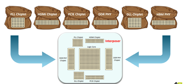
Farhang Yazdani, President & CEO of BroadPak, organized the tutorial, introduced the speakers, outlined the chiplet concept (Figure 1), discussed the role of interposers/substrates, and emphasized the advantages chiplets and advanced packaging offer, compared to single-die SoCs.
Yazdani also listed many chiplet information sources and addressed a frequently asked question in depth: What interposer/substrate) to use when? Here is a summary:
- Silicon interposers match the coefficient of thermal expansion (CTE) of chiplets, offer good thermal conductivity, allow L/S pitches of < 1 µm high aspect ratio through-silicon vias (TSVs), multiple redistribution layers (RDLs) and embedding of passives (RLC). However, they are costly (compared to organic and glass), limited in area, and very lossy at high frequencies (e.g. at ~ 60 GHz in 5G mm-wave applications).
- Organic interposers offer a significantly lower cost per area, can be much larger than silicon interposers, but limit L/S pitches to a few um today. However, they do not match the CTE of silicon – which may lead to cracking of thinned, large chiplets.
- Glass interposers can match the CTE needed, offer smooth surfaces, can be large, and are ideal for high-frequency designs. However, glass is an insulator – which is good if electrical insulation is needed, but their bad thermal conductivity makes them unsuitable for higher-power applications.
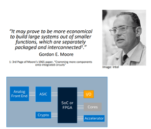
Krishna Settaluri from Blue Cheetah Analog Design, Inc., outlined how his company’s analog design tools, based on Berkeley’s BAG Framework, automate the generation of analog circuits, specifically designing physical layer I/O circuits (PHYs), compliant with Intel’s advanced interface bus (AIB). He developed the presentation together with David Kehlet from Intel and clearly showed that his team and Intel work together closely, to accelerate AIB market acceptance. To confirm the importance of chiplets, Settaluri showed a previously often overlooked statement from Gordon Moore (Figure 2) that predicted decades ago the need for these IC building blocks.
Sattaluri explained that lack of automation has contributed to making analog circuit design very time consuming and reuse of analog blocks difficult. This challenge has motivated Blue Cheetah Analog Design to develop an analog circuit generator. Together with proven Cadence tools, it increases analog designers’ productivity. To demonstrate this generator’s capabilities, he showed the layout of a 2-channel AIB PHY test chip, taped out for manufacturing in Intel’s 22FFL process.
Ramin Farjadrad, Marvell’s CTO Networking/Automotive PHYs, showed several design examples using silicon interposer, organic substrate, and fan-out wafer-level packaging (FOWLP). He outlined the strengths of each technology and compared their capabilities – e.g. using bit-rate (Gbits/sec), reach (mm) and power consumption (pJ/bit) – of AIB 2.0, HBM2e, HBI, Bunch of Wires (BoW) Base, AQlinkB on silicon interposers, then Kandou Bus, BoW-Fast, AQLinkP and XSR on an organic substrate. Farjadrad recommended BoW, an OCP/OSDA inter-Chiplet interface to use for silicon and organic substrates.

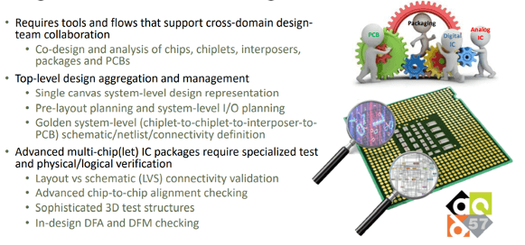
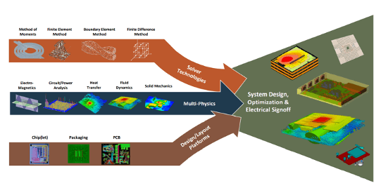
John Park, Product Management Director for Advanced IC Packaging at Cadence, reasoned why system and IC designers demand integration of chiplets in advanced packages and discussed some of the technical challenges for our industry. Figure 3 shows a high-level overview of important design tools/flows/methodologies needed, to optimize die-package-board co-design.
Park also explained why data about materials characteristics and accurate electrical, thermal, and thermal-mechanical modeling are essential to optimize performance, cost and reliability of multi-die designs. He showed how Cadence uses its proven as well as newly developed tools to address specific co-design challenges. In Figure 4, Park showed what kind of design tools/flows/methodologies Cadence is developing, to increase system and IC designers’ productivity and enable them to create sign-off quality inputs for manufacturing.
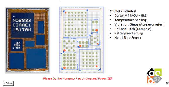
Jawad Nasrullah from zGlue emphasized that “Power is Everything” for IC designs, then outlined how zGlue’s ChipBuilder, their Active Silicon Interposer, and the Open Chiplet Initiative simplify multi-die IC design and help to save power. Figure 5 shows a design example with several dice on an active interposer.
Personal Comments
This tutorial was an important step towards addressing chiplet topics – special thanks to BroadPak’s Farhang Yazdani for organizing it. However, based on the most likely DAC audience – EDA developers and IC designers – most presenters focused on design topics and did not or only briefly address manufacturing, test, or material characteristics, all topics important for the 3D InCites readership. That’s why I am motivated again to get on my “soapbox” and ask for better cooperation between EDA & IC Design and manufacturing & test experts. Based on my 40+ years in this industry, I can assure you that all semiconductor supply chain members need to work together more closely, to accelerate market acceptance of innovations and reduce time to profit for all supply-chain members, from EDA developers to IC designers, to IC manufacturing and test experts to vendors of electronic systems.
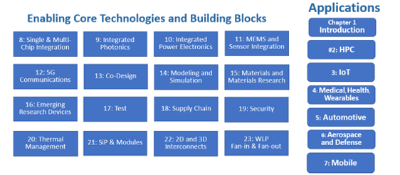
There is an excellent way to start bridging these gaps. I want to encourage you to read about it on SEMI’s website, then study the work of the pre-competitive technical working groups (TWGs), as they contribute to defining the Heterogeneous Integration Roadmap (HIR). Their efforts are sponsored by a number of major industry associations and address both important market requirements as well as development challenges. The TWGs focus on die-package-board co-design as well as manufacturing and test requirements of major applications. They talk to each other extensively, to synchronize development efforts with future market requirements. (FYI: HIR has replaced the die focused ITRS Roadmap because today’s and future challenges cannot be met with single die SoC solutions alone.) Figure 6 provides an overview of the currently active TWGs. The pointers in the following paragraph lead to much more information about HIR accomplishments, activities, and plans.
Please check/download/study for free:
- The 2019 edition of the Heterogeneous Integration Roadmap here
- he recordings of many Technical Working Group presentations here
- Please email Denise Manning at IEEE/IPS if you want to join/contribute to a TWG ~Herb


