

In my alliance management roles at electronic design automation (EDA) companies, I arranged many presentations to convey the benefits of EDA tools to IDMs, fabless IC vendors, and wafer foundries. Some of our EDA marketing people passionately presented their products’ strengths and demonstrated in-depth EDA knowledge. However, speaking fast, with a rich vocabulary, using many EDA acronyms, was not easy to understand for non-native English speakers, nor for manufacturing experts. The audience typically surrounded me after such a presentation and ask: “Herb, what did he/she say?” After summarizing the key problem(s) the tool was addressing, I recapped the key features/benefits within a few minutes. My audience responded with: “Very good tool! We’ll buy it.”
Having attended many of John Park’s presentations to EDA and/or IC design experts, I was concerned that he would show his vast EDA expertise and lose part of the materials, equipment, PCB and IC packaging experts attending this webinar. I would like to publicly apologize to Park for even thinking that he might make this rookie mistake, after 35 years in this field. Park speaks not only “EDA”, but also speaks fluently the language of the semiconductor manufacturing community!
Introduction
The International Microelectronics Assembly & Packaging Society (iMAPS ) organized this webinar and Brian Schieman moderated it. Schieman introduced the webinar and emphasized Park’s many years of experience. Park started his presentation by explaining why many applications now are better served with More than Moore (MtM) solutions than continued feature size shrinking (More Moore, MM).
EDA Tools for More than Moore Technologies
The title of Park’s presentation “This is not your fathers’ advanced semiconductor packaging …An EDA perspective” already hinted to a lot of progress at Cadence. The company started to address the need for streamlining PCB and package design with EDA tools in the early 1990’s. In the three decades since, Cadence has built a broad portfolio of EDA solutions to address system, board, package, and die design and co-design challenges. Park’s title is Product Management Director for IC packaging and cross-platform solutions. He leverages all these proven and widely used Cadence tools to develop flows and methodologies for solving planning, design, verification and especially integration challenges in today’s advanced packaging technologies.
MtM Designs Provide Subsystem Building Blocks
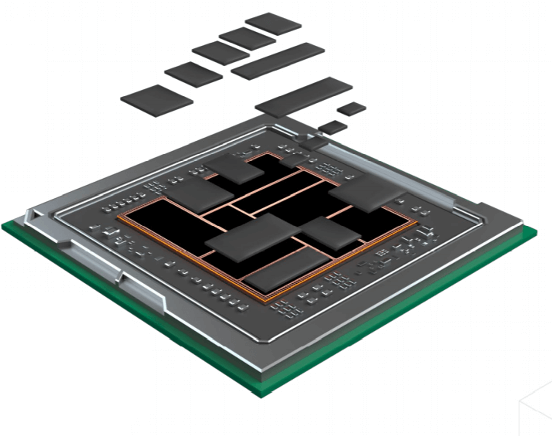
MTM designs can complement/enhance the value of MM solutions. Some people still wonder if MtM (a.k.a. multi-die IC) compete with MM (a.k.a. SoC) solutions. Park showed with Figure 1 that in particular, the rapidly emerging chiplets (bare SoC die) demonstrate and even amplify the synergy between MtM and MM solutions. Their combination enables modularity and they reduce development time, risk, non-recurring engineering (NRE), and lower system cost.
Park explained that wafer foundries are playing an increasingly important role in the IC packaging market, because, as interconnect geometries shrink, they require wafer-fab like equipment during assembly. He emphasized that just like foundries must provide process design kits (PDKs) to enable MM designs, the MtM supply chain partners need to offer package assembly design kits (PADKs) and reference design flows to make their customers and themselves successful.
PADKS are Important
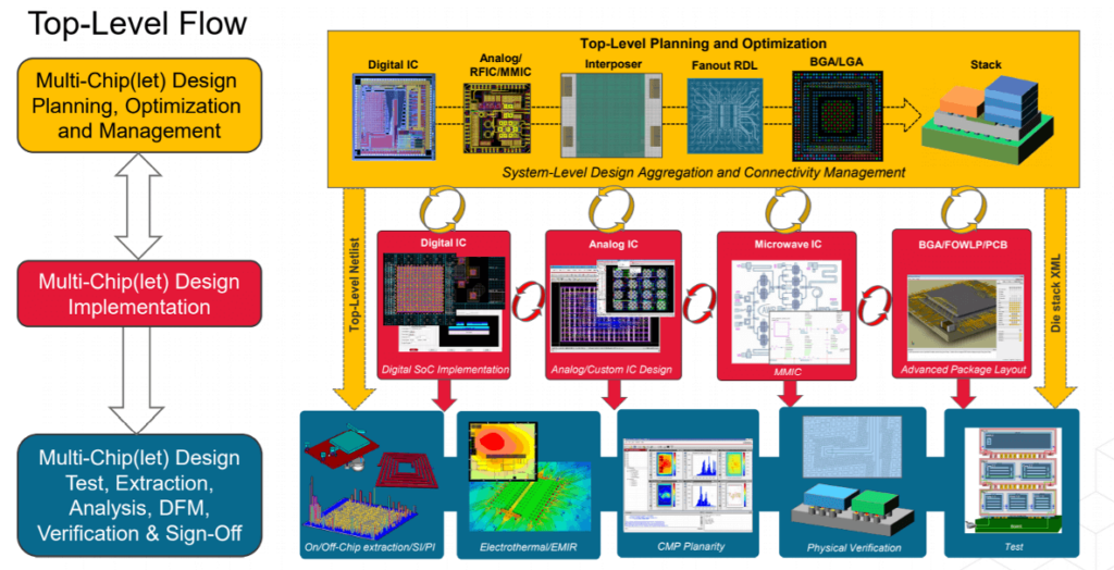
Figure 2 gives an overview of EDA tools deployed in MtM designs. They all need accurate inputs to produce accurate and meaningful outputs. Remember “Garbage in – Garbage out” arguments in the early days of computers! In addition:
- Large design teams, comprising experts for every design step, work simultaneously on a complex MtM solution. To assure the design team’s efficiency, down-stream and upstream data exchange is essential. Also, iterations within design steps and/or across multiple design steps are always needed to optimize a design. Cadence recommends the use of XML and Open Access formats to exchange data between tools.
- The characteristics of all MtM materials are needed for analyzing the electrical/thermal/mechanical/magnetic/optical interactions between MtM building blocks to assure high yields and reliability.
- Building blocks and interconnects between them need to allow testability to assure high yielding and reliable ICs.
- All building blocks need to first get modeled accurately to enable simulating their functionalities, interactions between building blocks and the performance of the entire MtM solution.
EDA Challenges and Considerations for MTM
While Figure 2 above only gives an MtM design flow overview, the example in Figure 3 gets into much more depth and shows some interactions and dependencies between design steps and tools.

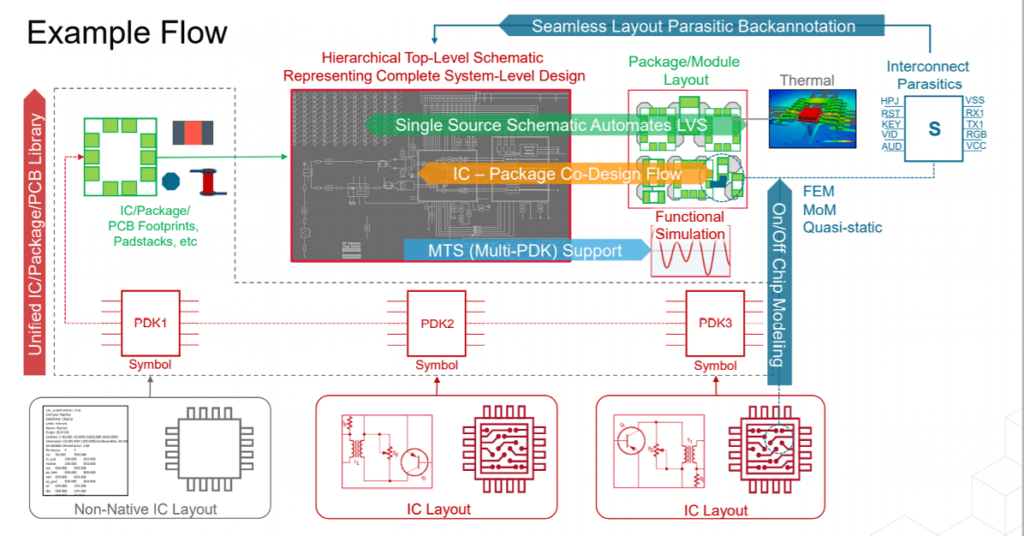
Park’s Figure 3 shows that a top-level schematic or netlist, with all MtM building blocks and interconnects, is needed to verify the entire design. In addition:
- To plan and optimize an MtM design early in the design process (a.k.a. do 3D Floorplanning), basic electrical, thermal, and physical information about every building block and all contact points is essential.
- To integrate 3rd party designs, accurate models – at the needed abstraction levels – are essential.
- To design and integrate heterogeneous functions (logic, memory, analog,…) in-house, PDKs of the relevant process technologies need to be available.
- The behavior of all package materials needs to be characterized over temperature, voltage, life-time, etc. and modeled. Then parasitics can be extracted and functionality, timing, coupling, power dissipation as well as power and signal integrity, can be accurately analyzed.
- Data exchange formats between design steps and for design transfer to manufacturing (GDS, Gerber,..) needs to be agreed upon between the parties.
- Instructions for how to test building blocks, partial assemblies and the final MtM solution need to be specified.
- Conclusion
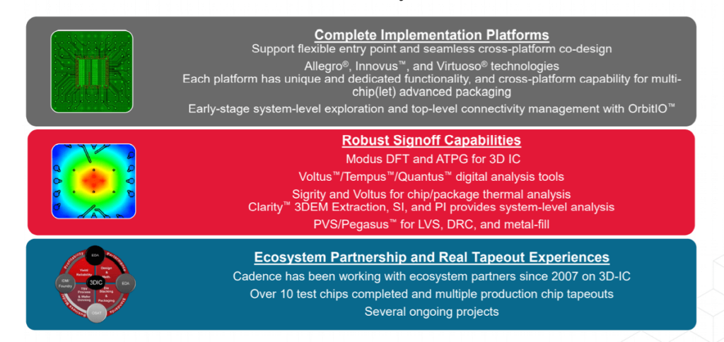
After conveying a lot of valuable information about MtM design challenges and how EDA tools address them, Park summarized the key value proposition and showed the names of Cadence’s many proven MtM design tools, in Figure 4.
After a brief Q&A, Schieman announced that two more iMAPS webinars with experienced speakers are currently scheduled: Andy Heinig from Fraunhofer ISS in Dresden will present on July 1, 9 am PDT. Laura Mirkarimi from Xperi in San Jose will present on July 15. You can register here, for iMAPS members at no charge. Members also can download Park’s slides, even listen to his and previous iMAPS webinars here. To become a member or sponsor, click here.
A Few Personal Comments:
It “only” took thirty years to bring the previously very segregated (sub-optimizing?) individual die // package // board // system design teams and their tools together to jointly plan and optimize system building blocks and entire systems. I have contributed to these efforts since 2008 and can assure you that the pace of MtM innovation is growing exponentially. Park’s presentation of Cadence tools and capabilities shows that benefits of MtM solutions are no longer only for large companies but also now reachable and valuable for medium size and smaller design teams.
After spending several decades contributing to today’s user-friendly and cost-effective ASIC design and manufacturing ecosystem, I am committed to spending some more time to help improving the MtM ecosystem. My primary focus is to encourage materials and equipment companies to accurately characterize their products’ capabilities to avoid the “Garbage in – Garbage out” surprises we have seen before. I realize that this will require major efforts – so was developing PDKs and reference flows at e.g. TSMC. If you, like many of my friends, see this foundation building as important, please join us!
Thanks for reading…Herb


