System-on-Chip (SoC) integrates ICs (by reducing the feature size) with different functions such as central processing unit (CPU ), graphic processing unit (GPU ), memory, etc. into a single chip for the system or subsystem. Unfortunately, it is more and more difficult and costly to reduce the feature size (to do the scaling) to make the SoC. Chiplet designs and heterogeneous integration packaging provide an alternative to SoC.
There are at least five different chiplet designs and heterogeneous integration packaging, as shown in Figure 1, namely, (1) chip partition and heterogeneous integration (driven by cost and technology optimization), Figure 1(a), (2) chip split and heterogeneous integration (driven by cost and semiconductor manufacturing yield), Figure 1(b), (3) multiple systems and heterogeneous integration with thin-film layer directly on top of a build-up package substrate (2.1D IC integration), Figure 1(c), (4) multiple systems and heterogeneous integration with TSV-less interposer (2.3D IC integration), Figure 1(d), and (5) multiple systems and heterogeneous integration with TSV interposers (2.5D and 3D IC integration), Figure 1(e). Figures 1(c) – 1(e) are driven by form factor and performance.
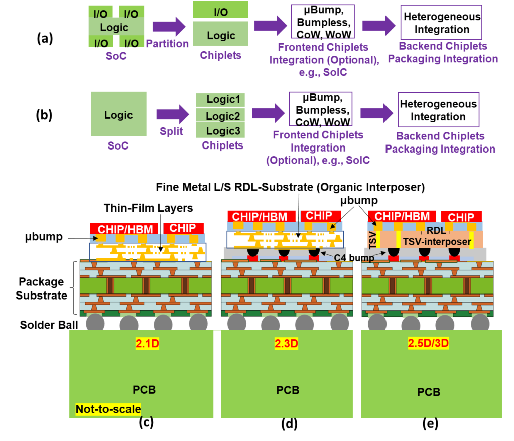
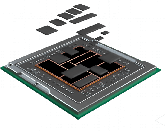
In chip partition and heterogeneous integration, Figure 1(a), the SoCs, such as the logic and I/Os, are partitioned into functions: logic and I/O. These chiplets can be stacked (integrated) by the front-end CoW (chip-on-wafer) or WoW (wafer-on-wafer) methods and then assembled (integrated) on the same substrate of a single package by using the heterogeneous integration technique. It should be emphasized that the front-end chiplets’ integration can yield a smaller package area and better electrical performance but is optional. For example, AMD’s EPYC shipped in 2019 and Intel’s Lakefield shipped in 2020.
In chip split and heterogeneous integration, Figure 1(b), the SoC, such as logic, is split into smaller chiplets, such as logic1, logic2, and logic3. These chiplets can be stacked (integrated) by the front-end CoW or WoW methods and then assembled on the same substrate of a single package by using the heterogeneous integration technique. Again, the front-end integration of chiplets is optional. For example, Xilinx’s FPGA shipped in 2013, AMD’s EPYC shipped in 2019 and Intel’s Lakefield shipped in 2020.
In multiple system and heterogeneous integration with thin-film layers directly on top of the build-up package substrate (2.1D IC integration), Figure 1(c), the SoC such as the CPU, logic, and HBM are supported by a build-up package substrate with thin-film layers. This is driven by performance and form factor and for high-density and high-performance applications. Unfortunately, because of the flatness of the build-up package substrate, the yield loss of the thin-film layers is very high and thus it is not in volume production.
In multiple systems and heterogeneous integration with TSV-less interposers, Figure 1(d), the SoC such as the CPU, logic, and HBM are supported by a fine metal L/S RDL-substrate (organic-interposer) and then on a build-up package substrate (2.3D IC integration). This is driven by performance and form factors and for high-density and high-performance applications. This technology is in small volume production and will take away some of the market shares from the 2.5D IC integration.
In multiple systems and heterogeneous integration with TSV-interposers (2.5D/3D IC integration), Figure 1(e), the SoC such as the CPU, logic, and HBM are supported by a passive (2.5D) or active (3D) TSV-interposer and then on a build-up package substrate. This is driven by performance and form factor and for extremely high-density and high-performance applications. Since 2013, products with this technology have been shipped by Xilinx, AMD, Intel, NVidia, Fujitsu, Graphcore, etc. In the future, this technology will be used more for extremely high-performance, high-density, and high-bandwidth products.

SoCs with chip scaling is and will be here to stay. Chiplet designs and heterogeneous integration packaging provide alternatives (options) to SoC, particularly for advanced nodes (smaller feature size) which most companies cannot afford. Also, chiplet designs and heterogeneous integration packaging may lower the semiconductor manufacturing cost of the products.
This blog post is from part of the introduction of Lau, J. H., “Recent Advances and Trends in Multiple System and Heterogeneous Integration with TSV-less Interposers”, IEEE Transactions on CPMT, Vol 8, August 2022, pp. 1271-1281.