
In the era of more-than-Moore, 3D IC is the new scaling approach adopted by the marketplace. Progress has been made throughout the semiconductor ecosystem in bringing 3D ICs designs to the mainstream, including design-for-test (DFT).
First came 2.5D Design-for-test
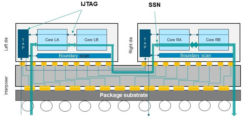
The industry got some practice for the challenges of 3D IC test with 2.5D designs, which are in production. 2.5D layouts, illustrated in Figure 1, have multiple ICs packaged side-by-side on a common interposer, which has more relaxed test accessibility than that of 3D stacking where dies are stacked on top of each other. 2.5D DFT involves a package-level 1149.1 compliant test access port (TAP), package-level boundary scan, and IJTAG support. The DFT methodology for 2.5D DFT is supported by IEEE standards (1149, 1687) and tools like hierarchical DFT and Streaming Scan Network (bus-based packetized test).
What’s New in design-for-test for 3D ICs?
For 3D IC logic test, we have these high-level considerations:
- Fully testing individual die at wafer level because some die pins are not available for probe by automatic test equipment (ATE)
- Choosing a technology for efficiently performing die-to-die test in the package. The interposer for 2.5D and through-silicon vias (TSV) or micro bumps for 3D stacking are examples of methods for inter-die connection. These die-to-die connections also need to support a repair mechanism to help recover yield loss.
- Choosing how to access any die(s) in the package for sufficient tests
- Automating failure diagnosis for inter-die and intra-die failures
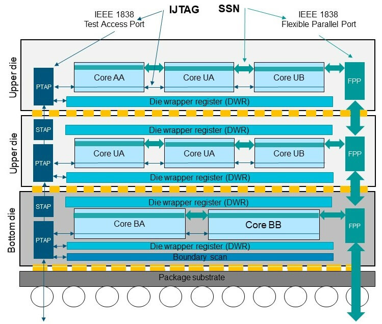
To define the standardized die DFT infrastructure (hardware and protocol) for inter-die integration, we have the newly-approved IEEE 1838 standard. IEEE 1838 allows test access to every die in a 3D stack. It has three important components: a mandatory serial port using primary and secondary TAPs to help inter-die communication, a die wrap register (DWR) to handle the die-to-die test, and a flexible parallel port (FPP) for transporting the scan data in/out of the dies in the stacking. Figure 2 illustrates the DFT setup for a 3D IC stacking.
Building a 3D IC DFT solution does not require design teams to start from scratch. At Siemens EDA, technologies like hierarchical DFT, IEEE 1687-compliant IJTAG network, and the new Streaming Scan Network (SSN) build a solid foundation for enabling 3D IC testing. In addition, various new technologies and compliance to IEEE 1838 and other standards are being developed to automate the DFT flow and test pattern generation.
3D stacking presents unique challenges for IC test, including:
- How to test each die at the wafer level where most pins are not available for probing
- How to reach embedded dies in the stack that communicate to the outside only through the bottom die
- How to handle the fact that usually, only the bottom die has a boundary scan
At the die level, DFT engineers can use die wrap cell analysis and insertion to make sure that the IOs not directly probable by ATE are instead controlled and observed by DWRs, the scan chains at the boundary of each die in the stack. The pins for TAP, FPP, clock, and power are designed with sacrificial PADs for wafer probe and discarded when dies are stacked together.
IEEE 1838 primary TAPs and secondary TAPs are built for die-to-die communication and the SSN packetized test delivery method with flexible bus width natively supports the most novel part of IEEE 1838, the FPP (flexible parallel port). The IJTAG network and language are used to operate and automate the whole DFT setup in the stack.

In the stack, a hierarchical DFT solution can retarget the test patterns (either BIST or scan pattern) created at the sub-die or die level to the package for testing. Die-to-die automatic test pattern generation (ATPG) is done by taking each die as a greybox wrapped by DWRs. Diagnosis based on hierarchical DFT is natively supported in Siemens EDA tools to identify the failures for inter-die and die testing.
In comparison, each die in 2.5D design may have a boundary scan, which requires package-level 1149.1 compliant boundary scan description language (BSDL) and BSDL based die-to-die test pattern generation. To accomplish this, a relatively simpler TAP is designed by adding a bypass feature to a traditional TAP. The TAPs are then sequentially connected with the bypass option. SSN can be implemented with flexible bus width to stream the scan data to each die and come out at the other side of the package. The scan test at the die level is done through hierarchical DFT where the test patterns are generated at the core or die level and retargeted to the package for testing. The IJTAG network connects to all the DFT IPs like TAP, boundary scan and SSN bus and automates the test setting and DFT network management.
While the technology for testing 3D ICs is partly available, 3D IC test is a moving target with more challenges that need to be addressed. Designers and DFT engineers will need more automated solutions, such as:
- Support for heterogenous die implemented with different DFT vendor solutions and dies with different technology nodes.
- Development of a repair mechanism to pass the inter-die connection failure info to the repair analysis engine in either 2.5D lateral or 3D stacking with redundant die-to-die connection in place, similar to that of memory BIST repair and an IO BIST.
For now, some important components for 3D IC are in place, available, and proven. Hierarchical DFT, an IJTAG network, SSN, and other technologies that are compliant with the new 3D test standards have already enabled the DFT designs for 3D IC. The development of automated solutions continues and involves players from across the ecosystem