
When I switched my focus from single-die SoCs to multi-die ICs, I had to learn a lot about IC packaging technologies. I paid thousands of dollars to attend 3DIC conferences, tutorials, and to purchase 3DIC books. This month (June 3 to 30, 2020) you can get up-to-date info about the state of More-than-Moore technologies at no charge, simply by attending ECTC 2020 online. I am impressed (and jealous!) as I see how easy it is now to access a broad range of packaging topics by viewing the many informative ECTC presentations. Register here and you can drink IC packaging know-how from a firehose, even from the comfort of your home. I suggest you look at the following sessions:
The Future of Interconnect technologies is Bright but also Challenging
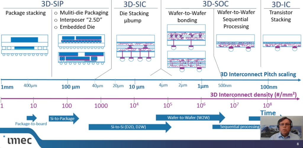
In the “Special Session 3DICs Past-Present-Future” of ECTC 2020 online, Eric Beyne, imec’s 3D-IC expert, projects how shrinking interconnect pitches will impact interconnect density and with it, improve performance per Watt and functionality per cm3 – see Figure 1.
Personal comments:
If you have traveled, like me, from 3µm transistors early in the 1980s to today’s development of 3nm devices, you can certainly imagine how much potential these new integration technologies can and will offer.
In the 1980s I saw our excellent circuit designers becoming desperate and our companies drowning in the rapidly increasing complexities of ASIC chips. Competitors, using electronic design automation (EDA) tools, were able to meet customers’ performance, cost, and delivery targets. HISTORY WILL REPEAT ITSELF! Beyne’s slide gives an excellent overview of why and how. It will hopefully encourage you to intensify your investment in design automation tools and broaden your team’s cooperation with EDA tools developers to assure the reliability of your designs and, equally important, make your chip integration methodology scalable in regards to the number of design starts you’ll be able to manage as well as the complexity limit for designs. In Figure 1, I also see the need for:
- Highly accurate (wafer-fab like) equipment
- Accurately characterized materials
- Extraction and simulation tools to assess thermal hotspots, the coupling between signals, and of course analyze thermal-mechanical interactions
Higher Packaging Densities Increase Electrical-thermal-mechanical Challenges
In Session 12.1, Chi-Wei Wang, from Taiwan’s National Tsing Hua University, addresses thermal-mechanical interactions. He presents how the coefficient of thermal expansion (CTE), Poisson’s Ratio, and Young’s Modulus determine how silicon die, interposer(s), organic substrate(s), copper through-silicon vias (TSVs) and redistribution layers (RDLs,) molding compound, and other materials behave over temperature. These variables impact how the different materials interact with each other – electrically, thermally, and mechanically – when packed together in a multi-die IC. Figure 2 illustrates this topic.
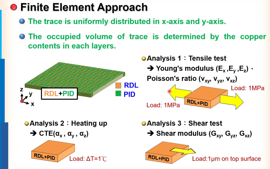
(Source: ECTC 2020, Session 12, 1. presentation, by Chi-Wei Wang, Microsystems Mechanical Design & Reliability Analysis Lab, National Tsing Hua University, Taiwan)
With increasing design complexities and a variety of materials, hands-on engineering experience will no longer suffice to create reliable ICs. Only accurate material characteristics, fed into EDA tools, will be able to keep pace with the increasing number of challenges.
Personal comments:
I recommend that you also read Francoise’s blog about the visionary keynote TSMC’s Doug Yu gave at ECTC 2020 online.
Above, and in some of my previous blogs, I try to convey that I am extremely focused on getting accurate inputs for EDA tools from materials and manufacturing/test experts. Only accurate inputs and user-friendly design tools can enable chip, package, and system designers to fully utilize all the hardware capabilities IC packaging experts are developing.

Why do I say this? In the late 1990’s I spent three years of my life making PrimeTime a widely useable, static timing analysis EDA tool. It eliminated the dreaded “timing closure” problem for ASIC designs. My team enjoyed excellent cooperation from the library development teams at the top 10 IDMs as well as at TSMC. Their accurate inputs enabled PrimeTime to precisely identify race conditions, calculate critical path timing, set-up and hold violations, etc. to practically eliminate re-spins because of timing errors. Synopsys’ open-minded software development team worked with my team to make PrimeTime an accurate, feature-rich and user-friendly design and verification tool for ASIC complexities of a few Million gates in 1998 and ‘99. More than 20 years after we integrated PrimeTime into many companies’ IC design infrastructures, it still has about 90% market share and enjoys the “golden timing sign-off tool” status for multi-billion gate designs at TSMC, other wafer foundries, and most IDMs. If you are or have been involved in ASIC design, you’ll value the powerful combination of accurate inputs and user-friendly EDA tools and, hopefully, will support my frequent requests for accurate materials characterization data and close cooperation between materials/manufacturing experts and EDA vendors to enable characterization and design methodologies that produce accurate results, avoid costly re-spins and/or poor production yields.
As I outlined in a previous blog, the Heterogeneous Integration Roadmap (HIR) efforts address in Chapters 13 and 14 the need for much closer cooperation between EDA / Design and manufacturing/test experts.
In the Special Session HIR, Chris Bailey from the University of Greenwich and Chair of HIR Chapter 14 outlines in Figure 3 how today’s “cooperation” between design and manufacturing needs to change to keep pace with emerging challenges.
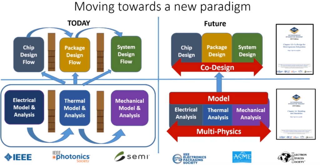
(Source: ECTC 2020, Special Session HIR, Presentation by Chris Bailey, University of Greenwich and Chair of HIR Chapter 14)
Personal comment: Thank you, Chris, for amplifying my message!
Thanks for reading…Herb


