

In Austria, where I grew up, homes get passed on from generation to generation. Like many Austrians, I had a set of tools to repair plumbing, electrical, heating, and other equipment, to keep our old home comfortable. As a proud handyman, I took all my tools with me, when I moved to California in 1983. This move was smart – but bringing my metric wrenches was not! In the U.S. inches, feet, yards, etc. rule. While Europe follows the metric standards and simply adds or drops zeros, when dealing with dimensions from nanometers to kilometers, the U.S. keeps children and adults busy with calculating, e.g. how many inches are in 4 ¾ yards? I am not trying to revolutionize the American Way of living; I am only giving an example of how agreed-upon good practices and standards can impact productivity and avoid costly mistakes.
The Importance of a Roadmap
With this blog post, I want to encourage readers to contribute to the ongoing pre-competitive joint development efforts and contribute to one of the Heterogeneous Integration Roadmap (HIR) Technical Working Groups (TWGs). They are identifying challenges to be addressed and discussing possible solutions. These TWGs lay the groundwork for best practices and eventually standards for planning, design, assembly, and test of homogeneous and heterogeneous building blocks and techniques to pack them into multi-die ICs (a.k.a. 2.5D/3D-ICs). In fact, you can tune into the Virtual Heterogeneous Integration Roadmap Workshop as part of ECTC 2020. Register and gain access here.
From 1980 to 2008 I was focused on system-on-chip (SoC) design and manufacturing challenges. The National Technology Roadmap for Semiconductors (NTRS) and, starting in 1993, the International Technology Roadmap for Semiconductors (ITRS) gave the companies I worked for and our entire supply chain roadmaps to synchronize developments of manufacturing and metrology equipment, materials, process technologies for dice and packages and other essential enablers for SoCs to meet market requirements timely and cost-effectively.
From Moore’s Law to More than Moore
In 2008 my focus changed to multi-die ICs because continued feature-size shrinking was becoming much less attractive for many applications. I admired the custom multi-die solutions of integrated device manufacturers (IDMs) and outsourced semiconductor assembly and test (OSATs) service providers, e.g. System-on-Package (SoP), System-in-Package (SiP) and technically similar multi-die solutions but noticed that their market acceptance was limited. My 25+ years of contributing to building the ASIC ecosystem taught me that closer cooperation between the design community — developers of Electronic Design Automation (EDA) tools, Intellectual Property (IP) building blocks and designers of ICs — with process development, manufacturing, and test experts was needed, to make the multi-die IC business model more cost-effective and scalable. I started consulting with several industry organizations (GSA, SEMATECH, Si2, ESD Alliance, SEMI) and my communications partner 3D InCites, to encourage industry-wide cooperation for pre-competitive multi-die IC development. When the Heterogeneous Integration Roadmap (HIR) efforts replaced the ITRS in Spring 2017, I got the opportunity to contribute to the Technical Working Group for co-design (TWG #13).
The need for Heterogeneous Integration
Multi-die ICs (a.k.a. 2.5/3D-ICs) enable dice containing logic, memory, analog, RF, MEMS, and other functions, all manufactured in the most suitable process technology, to be combined in an IC package – to significantly reduce PCB space. With it, a significant part of the value creation moves from PCB and dice to the package and its components. More dice in an IC means much larger functionality as well as higher power density. Both require EDA tools to accurately model and analyze electrical, optical, thermal, magnetic, mechanical, and chemical characteristics and interactions of the densely packed components – to assure reliability.
Just in case you did not have the opportunity to study the 2019 edition of the HIR yet, allow me to briefly introduce this important document to you. HIR efforts encourage industry-wide cooperation for building a cost-effective and scalable ecosystem. The IEEE Electronics Packaging Society, the Electron Devices Society, the IEEE Photonics Society, ASME, and SEMI are HIR sponsors and encourage their member companies to contribute to one or more TWGs.
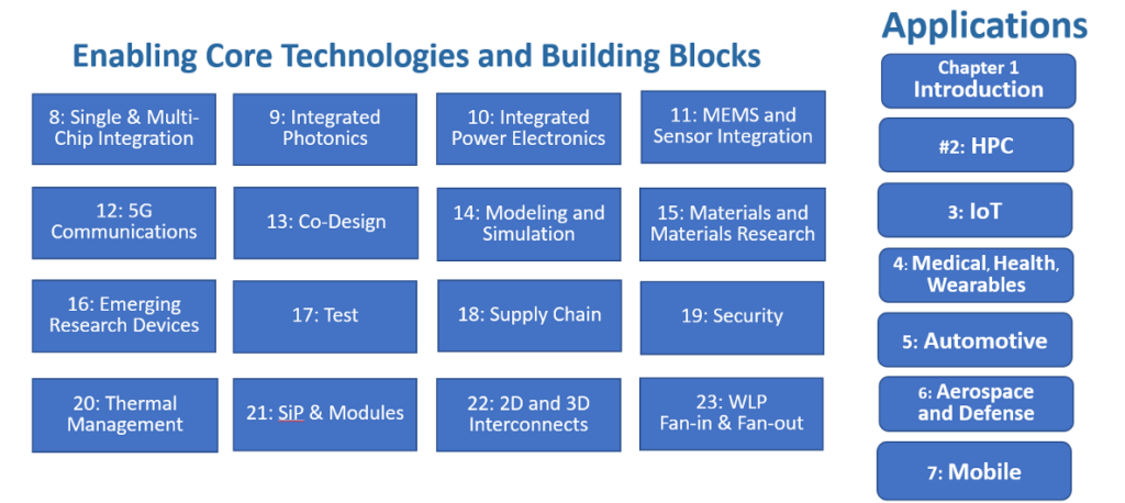
Heterogeneous Integration Roadmap – Overview
HIR Chapter 1 highlights the importance of high-tech companies, measured by market capitalization. In 2006 Microsoft was the only high-tech company in the top 10 worldwide, according to The Economist and Statistica. In 2019 Apple, Microsoft, Amazon, and Alphabet ranked #1 to 4, Facebook, Alibaba, and Tencent Holdings ranked #6, 7, and 8. In my opinion, there is no better way of emphasizing the importance of high-tech companies than seeing where people put their money. All these companies rely on semiconductors to run their equipment and provide services. To shoulder this burden and assure continued success, the semiconductor industry, now dis-aggregated into many highly focused companies, needs to look ahead jointly, project future customer requirements as well as plan and execute accordingly.
Above mentioned industry organizations and their members contribute to the HIR efforts. TWGs #2 to 7 focus on major semiconductor applications. They analyze these applications’ current and likely future requirements and project which capabilities will be needed longer-term (in the next ~ 15 years) to meet future demands with the right semiconductor technologies. At regular intervals, they hold worldwide meetings. TWGs #2 to 7 communicate their findings and projections to the TWGs #8 to 23, define the efforts needed to meet future market needs and discuss which developments of core technologies and building blocks are required for the long-term success of our industry.
The Importance of EDA Tools
During my ASIC Marketing years, I had to watch helplessly the decline of two of my employers, primarily because top management did not believe the productivity increases and unit cost reductions EDA tools offer. That’s why I Joined EDA companies for several years, then founded my own company (eda2asic) in 2002 with the mission to bring EDA tools developers closer together with ASIC manufacturing/test experts and their management.
![[err-ad-fallback-title]](http://www.3dincites.com/wp-content/plugins/a3-lazy-load/assets/images/lazy_placeholder.gif)
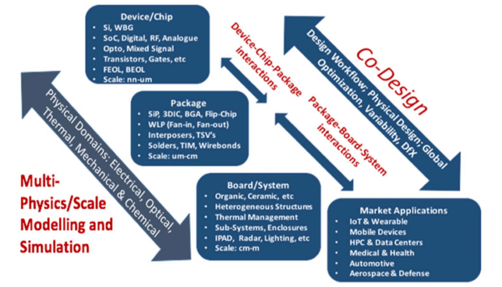
TWGs 13 (co-design) and 14 (modeling and simulation) in context with the semiconductor ecosystem
Figure 2 shows many devices – chip – package – board – system topics engineering teams need to consider for achieving cost-effective multi-die IC solutions in a timely manner. Figure 2 also shows that accurate modeling and simulation of package components and die-level building blocks (a.k.a. Chiplets) is needed as inputs for EDA tools to achieve reliable ICs.
Personal comments
During my ASIC years, I learned how valuable EDA tools are. My first ASIC had 500 gates and our engineering team managed manually (and slowly) to get such gate arrays to work. However, when ASIC complexities increased to almost a million gates, it became mandatory to purchase good commercial design tools, to implement customers’ requirements in these large ASICs. Today’s single-die SoC designs are comprised of billions of gates and the design teams manage to get such complex designs right, often the first time, and can avoid time-consuming and costly re-spins – thanks to EDA tools.
Multi-die ICs can contain several multi-billion gate logic designs, large memories, analog / RF dice, and other heterogeneous functions. These complexities, combined with today’s time to market and unit cost pressures, demand the use of EDA tools and close cooperation between EDA tools developers and IC manufacturers, to assure high productivity and user-friendly EDA tools for modeling and simulation of building blocks as well as planning, design and verification of entire multi-die ICs.
Multi-die ICs are an important steppingstone from today’s single-die components to a much higher value (sub)system-level building blocks. Companies like AMD, Intel, Nvidia, and others have already demonstrated competitive and highly profitably multi-die ICs and are being trailblazers for multi-die IC technologies. Jump onto the multi-die IC train and enjoy the ride!
Thanks for reading…Herb


