
3D very large system integration (3D VLSI) has many aliases. This high-density approach to 3D system integration first appeared on the scene as monolithic 3D (M3D), or as Leti dubbed it: sequential 3D. In 2014, the French research institute officially introduced it as CoolCube™ because this version of the technology addressed the thermal issues that plagued early versions of M3D. This paved the way for implementing it as a viable alternative to traditional scaling at the system level – aka true 3D VLSI.
I caught up with Severine Chéramy, 3D Business Development and ITR 3D director at CEA-Leti, when I attended the MEMS, Imaging and Sensors Summits in Grenoble. We talked about the progress of 3D VLSI and about an upcoming workshop that you might want to attend if you want to be part of this exciting ecosystem.
Why 3D VLSI?
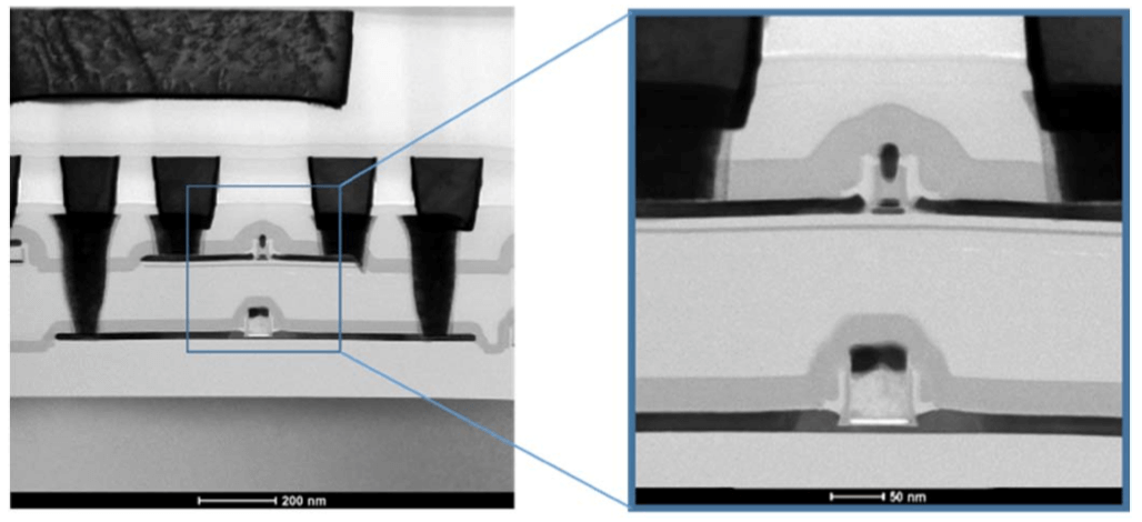
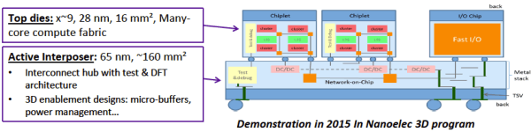
Formerly known as “active interposer” technology, 3D VLSI integrates advanced node ICs of various functions on top of mature node ICs that have minimal function.
For example, a 28nm fully-depleted, silicon-on-insulator (SOI) device is stacked onto a 65nm die that performs only power management functions, explained Chéramy. A photonic device and/or high bandwidth memory (HBM) stacks can also be integrated into the system (Figure 1).
“When you think about VLSI, you think about the system, not only the technology,” explained Chéramy. “You think of the capability of 3D using hybrid bonding to achieve high accuracy.”
Chéramy reminded me that I was among those who had scoffed at the “active interposer” term. Thus the term, 3D VLSI, was adopted. (I had no idea I was that powerful an influence).
The Difference between Sequential 3D and 3D IC
Elaborating further, Chéramy said the difference between sequential 3D and traditional 3D IC stacks can be boiled down to density. Sequential 3D density is in the nanometer range and uses layer transfer and hybrid bonding technology. 3D IC density is in the micrometer range and uses more traditional stacking methods, such as through silicon via (TSV) interconnects to stack die-on-die.

Widespread Interest In 3D VLSI
In the beginning, Leti was very much alone in the 3D VLSI effort, noted Chéramy. But high-density stacking has been gaining interest year-over-year, and in the last year, the concept of integrating sequential 3D and 3D ICs in one system is becoming more popular.
She cited applications that need a high quantity of memory embedded near to the computing system itself as great candidates for 3D VLSI solutions. This is generating interest among fabless companies, such as Qualcomm, as well as those specializing in gaming technology.
Learn More
On October 16, 2018, CEA-Leti and Qualcomm will once again host a 3D VLSI Open Workshop as a free satellite event to the IEEE S3S Conference.
According to Chéramy, Qualcomm was the first promoter of 3D sequential technology but knew it needed an entire ecosystem built around it to succeed. So in 2014, they partnered with Leti to host an annual Open Workshop initiative. Attendance is always free, and papers are invited from the ecosystem. The details for this year’s event are here.


