
When is an active die not an active die? When it’s an active interposer, of course!
Ever since Nicolas Sillon, former head of CEA Leti’s 3D Integration program, first talked about the research institutes’ work with interposer technology for 3D integration, the term “active interposer” has sparked controversy and begged for definition. Sillon differentiated active interposers from 3D ICs as having only low-cost mature technology rather than high density advanced nodes. But that was still rather vague to me. So when the topic came up again this year at the 2014 European 3D TSV Summit, I asked Leti’s new 3D lab manager, Séverine Chéramy, to expand on the definition.
Chéramy explained that at CEA–Leti, where 3D integration work focuses on silicon interposers for high performance computing, mobile, and heterogeneous applications, active interposers are distinguished from active die in that they have very basic devices designed into the silicon that allow the interposer to do more than just provide interconnect, but also add performance enhancement.
Pascal Vivet, project manager on 3D design, added to the explanation, noting that the active interposer is “not a real chip; it’s an almost empty device, thus ensuring high yield and low cost for large size interposer”, while including efficient Interconnect and power management provided by capacitors. “It brings smartness to the interposer so that the whole system is smart,” he explained.
Next on Leti’s interposer roadmap is what Patrick Leduc, 3D Program Manager, defined as an “optical interposer” with integrated Si photonics. He broke down the three interposer categories as “metallic, active and optical” and explained when to use which.
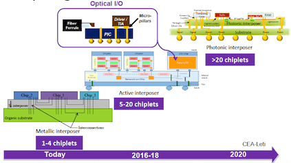
Leduc explained that for high bandwidth computing, standard (metallic) interposers are limited by horizontal electrical connections over 2-3 Gbps. Active and Si photonics enables denser integration with improved scalability. In basic terms, he said a metallic (or standard Si interposer) is optimal for 1-4 chiplets. Active interposers are best for an intermediate number of cores (5-20 chiplets) and optical (photonics) interposers will be relevant for many-core systems.
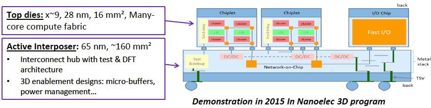
To further establish the difference between active die and active interposers, Chéramy offered an example of a demonstrator device featuring six high performance (28nm FD SOI) ‘chiplets’ interconnected on a 65nm node interposer that has an interconnect hub with test and design for test (DfT) architecture built in. The interposer features network-on-chip functionality and signal repeaters that create a high performance link between the chiplets and the interposer. “Higher performance needs will require active CMOS inside the interposer,” she explained.
The demonstrator is part of IRT NanoElec 3D program managed by Chéramy. It was first launched in April 2012 by CEA-Leti, ST Microelectronics, and Mentor Graphics, and is open to external partners. The program objective is to develop a generic and holistic platform for 3D integration design technology characterization and to apply it to applications prototyping. Chéramy said the focus is to have one demonstrator per year that includes process developments for 3D interconnections, development of design tools and test methodologies at the wafer and system level; validation on demonstrators and prototypes; and cost evaluation at the system level, rather than unit cost. They are also looking at thermal management issues.

“First we have to define the real (thermal) issue, which can be different with each application,” she explained. “Do we need a heat spreader? Microfluidics? Is it a design issue? The plan is to integrate a thermal sensor into each demonstrator and do thermal mapping to answer these questions.
Tackling thermal issues is also a critical part of what Pascal Vivet’s 3D Design group is focused on in collaboration with EDA vendors Atrenta, Docea Power, and Mentor Graphics. The group is working to design a complete 3D design flow and coordinate various CAD aspects. The 3D design flow includes 3D exploration, 3D Implementation, and 3D Sign-off.
With Atrenta, they are working on RTL exploration for system level partitioning. “Where should you put the memory, or the CPU?” he explained. “You have to consider performance, area, thermal power, etc. If it’s a system with lots of function should it be 2D, 2.5D, 3D? With a tool that gives a 3D view we can take exploration to simulations and get feedback on the functions.” This way, decisions can be made about what technology goes where in a full 3D stacks, such as where to put the TSVs and the microbumps.
Docea Power is providing CAD tools for system-level exploration of power and thermal, which can be used by architects for design exploration. Vivet explained how Docea’s tools are being used to create a virtual platform for simulation to model a full system including a 3D stack. This is particularly useful for power and thermal simulations. This, in conjunction with work with Mentor Graphics to develop physical design and implementation tools will pave the way for thermal management solutions. Mentor’s sign-off tools provide final verification of the power budget and thermal budget within the stack. This is significant because “We can’t fix thermal issues until we validate them,” noted Vivet.
As previously mentioned, Leti’s focus for its 3D interposer technology is not consumer applications. Gilles Simon, who heads up the 3D packaging lab, said the target for all this heterogeneous integration work with Si interposers is high performance computing, medical and biomedical devices, and advanced CMOS imaging devices.
Examples of recent projects include figuring out how to managing internal stress, which is a major issue for wide-dimension interposers. Simon says they’ve been successful in developing a protocol for to manage this stress that included different coating processes, material deposition, thickness, and a compensation layer. Additionally, his team has been instrumental in improving imaging functionality for backside illuminated CMOS image sensors (BSI CIS) with ST Microelectronics, as well as the development of an active heart implant that serves as a defibrillator rather than a pacemaker by means of an embedded accelerometer.
Simon explained that the ultimate goal of all these various 3D-focused projects and roadmaps culminates in Open 3D, wafer services provided by Leti that integrates the aforementioned off-the-shelf 3D building blocks into prototypes. The proposal targets R&D and product development teams in industry and academia and thereby serving Leti’s overarching mission which, simply put, is to create and transfer innovation to its industrial partners. ~ F.v.T.


