
Tomorrow’s the big 3D day, but today’s keynote from Nicolas Sillon of CEA Leti on “Silicon Interposer: Much More than a Piece of Silicon” solidified the concept for me that interposers are not merely a bridge to 3D, but have a future all their own in parallel to 3D ICs.
Sillon charted a course for the technology, looking far into the future (as research scientists will do) where silicon interposer technology moves from what he called “more wires” to “more than wires” to “much more than wires.”
XIlinx’ FPGA configuration is a classic example of silicon interposers as more wires – allowing for increased interconnect density. There is already a ‘generic technology’ in this space. 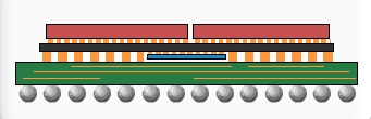
 “More than wires” refers to the addition of passive integration to create a “smart interposer”. He cited work by Ipdia as an example, which has developed 3D integrated capacitors that allows for high value capacitance in the interposer, thereby achieving a 40% area decrease and 35% height decrease. The demonstrator is for a medical application, where size and thickness is very important.
“Much more than wires” involves putting transistor technology into the interposer to create an “active interposer”. What differentiates this from a 3D IC, explained Sillon, is that it uses low-cost mature technology rather than high density advanced nodes, containing some parts of an SOC that does not require shrink or aren’t shrinkable. “This allows us to embed external functions that are today in a separate package,” he noted.
Leti’s vision for a silicon chip 10 years out? Sillon showed a schematic of a heterogenous device built on a silicon interposer that included stacked advanced logic and memory, passives, stacked DRAM or Flash, moving parts (MEMS?) optical I/Os for communications and a ‘smart’ thermal management system.

Ironically, Sillon pointed out that the same challenges involved in realizing this vision: high cost, incompatibility with the supply chain, not repairable, difficult to test, and lack of reliability, are the exact same as what we were facing a few years ago when silicon interposers were being developed. “We’ve decided to forget the drawbacks and focus on the fact that this integration is small, fast and power efficient. It’s a good target to drive the 3D integration toolbox development.” he said. “We don’t have to have all the bricks to make products and money with 3D integration. There are lots of intermediate stand-alone products and business opportunities along the way.”
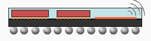
Future challenges that Leti is prepared to take on include package-to-package and chip-to-chip optical links, targeted for 2016 and 2020 respectively. “We think interposers can be a vehicle for that.” he said. Even further out – around 2020 – he talked about fabricating electronics with molecules taking us “beyond CMOS”. “If we imagine one day, this kind of thing emerging as a companion to CMOS; there’s a link between what we do today in the foundry and what we can do with molecules in the future,” he said,
In conclusion, “2.5D is just the beginning of a long story in parallel to 3D IC emergence.” explained Sillon “There are lots of things to do on an interposer. Passive integration on an interposer is already started, and we really think evolution toward active interposers will play a big role in mobile applications.” He added that future work on photonics and “Beyond CMOS” will add to the 3D toolbox.


Regarding #3
Miles – I’m inclined to agree with you. Anything else gets to confusing. Now to convince the rest of the industry!
Calling a piece of silicon with active devices a “much more than wires interposer” just leads to confusion. It doesn’t matter whether it is manufactured in leading edge technology or not. Stacking silicon with active devices is by definition a 3D IC stack, not surprisingly with all the added benefits and difficulties of true 3D IC stacking.
Regarding #1
Klaus – I posed the question, isn’t an “active interposer” just an active chip – ie 3D IC? I was told that it refers to a low density device. I got a similar answer from imec about the difference between 2.5D and 3D interposers from Eric Beyne in an interview that I posted a few weeks ago here.
I’d be interested in your perspective on this too. Will the industry settle on a set of consistent terms?
IMHO:
If it has transistors of any kind, it shouldn’t be called an interposer.
If it is only used for interconnect, that is a “standard interposer”.
If it incorporates non-transistor devices (capacitors, etc.), that is a “passive interposer”.