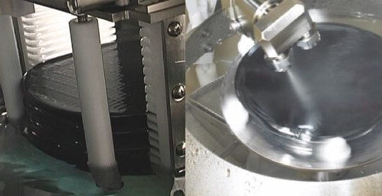
Temporary wafer bonding processes were initially developed for enabling three-dimensional (3D) stacked integrated circuits (ICs). For example, dies can be...
NMP is an abbreviation for N-methyl-2-pyrrolidone (other synonyms are 1-Methyl-2-pyrrolidone and 1-Methyl-2-pyrrolidinone) (Figure 1). NMP has proven itself as an...
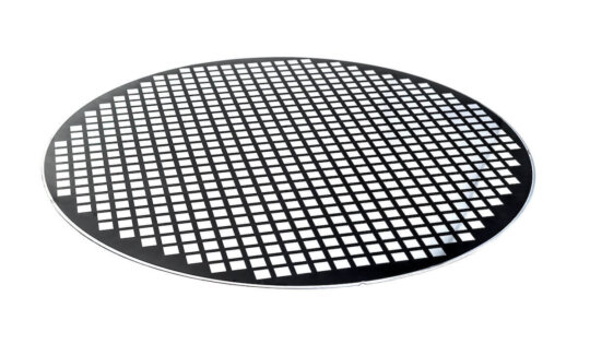
The constant demand for miniaturization, added functionality and increased performance of electronic devices systematically drives higher integration by adding more...
SABRE® 3D is a next-generation electroplating product designed to meet leading-edge production requirements for advanced packaging applications. This product leverages proprietary...