Temporary wafer bonding processes were initially developed for enabling three-dimensional (3D) stacked integrated circuits (ICs). For example, dies can be stacked on top of each other using die-to-wafer stacking to create 3D IC stacks. Through-Si vias (TSVs) and microbumps are used to interconnect the finished dies. These techniques require the processing and handling of ultra-thin substrates, which have been enabled by the first-generation of temporary wafer bonding solutions. By using these technologies, the thinned device wafers on a carrier can now be processed through successive multiple backside process steps. At the end of these processes, wafer de-bonding solutions allow the carrier to be separated from the device substrates with only a minimum of stress.
However, recent advancements in assembly and packaging brought along new challenges for temporary bonding. An example is the rise of fan-out wafer-level packaging (FOWLP), a flavor of wafer-level packaging (WLP) technology that answers the demand for more functionality, increased I/O count, smaller form factor and cost reduction. With FOWLP, a redistribution layer (RDL) is created to re-route the die connections (I/Os) to the desired (bump) location on top of the die surface. The RDL is created either prior to or after a wafer over-molding step. The function of the epoxy mold is to protect the individual components and hold them all together.
The processing of these reconstructed over-molded substrates is putting new constraints on temporary bonding. One of the main challenges is stress holding, related to the large mechanical property mismatch between the over-molded substrate and the carrier. Temporary adhesive solutions must now cope with high and varying stress levels throughout the various process steps while trying to maintain the wafer geometry (i.e., warp and bow).
Meeting the Requirements of a Novel FOWLP Technique
In this article, we introduce advanced molding materials and new temporary bonding and de-bonding solutions. These solutions have been developed to answer the needs of a new flavor of FOWLP developed at imec — its flip-chip on fan-out wafer-level packaging (Figure 1). More specifically, the challenge was to realize extremely low die shift in combination with low wafer bow and warpage — after wafer over-molding.
Although specifically developed for this new FOWLP flavor, the technology may open new horizons for the processing of over-molded substrates. For example, if low-warpage can be achieved, these overmolded substrates can access more standard silicon back-end-of-line process equipment, eliminating the need for dedicated toolsets that can handle large wafer bow.
Prior to giving more details on the new molding and de-bonding technologies, we will briefly summarize the major steps of the flip-chip on FOWLP technology — as these have set the requirements for the new technology.
Flip-chip on FOWLP: A Quick Summary
Imec’s flip-chip FOWLP technology was developed to push the boundaries of conventional FOWLP solutions in terms of chip-to-chip connection density. Using this FOWLP approach on 300mm wafers, ultrahigh interconnect density with 20µm pitch is now within reach. The technology is particularly attractive for mobile applications as it enables a cost-effective wide I/O memory-to-logic interconnect in a very small form factor. But it may also become an enabling technology for heterogeneous integration targeting high-performance applications.
Flip-chip on FOWLP basically uses a mold-first approach: dies are first assembled on a temporary carrier, followed by wafer over-molding. In the final stage, the redistribution layer is created, and connections are made. But contrary to standard mold-first approaches, dies are now over-molded after the formation of the chip-to-chip interconnections. This way, chips are already interconnected before being shifted during the over-molding process.
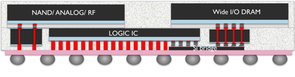
The imec team demonstrated the feasibility of this approach by using a test vehicle that is composed of seven individual (dummy) chip components: wide I/O DRAM, Flash memory, logic, two through-package vias, and two Si bridges. The interconnecting Si bridges and the through-package via chips are key components to realize the high-density connections. Through-package via chips are Si dies with through-Si vias (TSVs) and bumps of 40µm pitch. The Si bridges have bumps of 40µm and 20µm pitch. These components form a bridge between the functional dies (e.g. the logic and memory die), enabling ultrahigh chip-to-chip interconnect densities with a 20µm bump pitch.
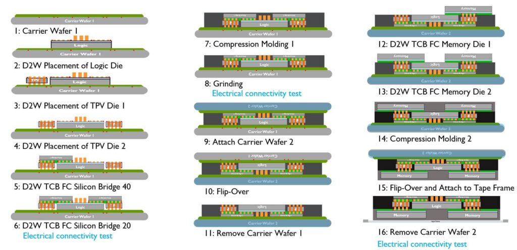
In a first step of the flip-chip on FOWLP assembly process flow (Figure 2), the through-package via and logic dies are placed on a carrier wafer with a temporary bonding layer on top. Next, the Si bridge (with 40µm and 20µm bump pitches) is attached using a thermocompression bonding (TCB) step. In this process step, bumps with 40µm pitch are attached to the through-package via side and to the left side of the logic die. The 20µm pitch bumps are attached to the right side of the logic die. In the next step, the wafer is over-molded by a liquid mold compound. Afterward, the Cu pillars are exposed through grinding so that later, they can connect with the RDL. After flipping the thinned wafer to a second carrier and removal of the first carrier, the memory dies are assembled using flip-chip technology. A second wafer-level molding and removal of the second carrier complete the process flow. The result is a complete package of only 300-400µm thickness (excluding the solder balls).
Finding the Right Adhesive and Mold Materials
Throughout the assembly flow, two temporary carrier substrates are being used. Their role in the assembly process puts very specific requirements on the adhesive material that is used for temporary bonding, and on the release material used for de-bonding.
The main role of the first carrier system is to assemble chips (i.e., the through-package via and logic dies) with extremely high inter-die alignment precision: +/- 3µm die-to-carrier placement accuracy is needed to allow for 20µm bump pitches. Such an accurate placement can be obtained by incorporating alignment marks into the carrier and die designs. The first adhesive material must, therefore, be sufficiently transparent to enable pattern recognition for alignment.
Next, the imec team looked for a material that allows the dies to be placed at room temperature. At this temperature, thermal expansion issues can be eliminated, enabling more precise die-to-carrier alignment. At the same time, the adhesive must be able to withstand higher temperatures during a subsequent TCB die-to-wafer bonding step (see steps 5 and 6 in Figure 2), and the material must be capable of maintaining the dies in place during the wafer over-molding step. In the end, the adhesive material should also allow carrier-one debonding while maintaining a minimum wafer bow.
The main role of the second carrier is to enable the removal of the first carrier system. When this is removed, the front-side of the original devices can be re-accessed for testing and further processing. A major requirement for this second carrier system is, therefore, to enable the selective removal of the first carrier, without damaging the reconstructed wafer or increasing the warpage.
Die shift, wafer warpage, and bow can also be influenced by the mold material and wafer over-molding techniques. The assembly flow for the flip-chip on FOWLP involves two separate mold steps. A first over-molding step takes place after the silicon bridge is placed; a second after the memory die is flip-chip attached. It will be key to identify the right combination of temporary bonding and mold materials and processes to guarantee a low wafer distortion and die shift after molding.
The Outcome: Record Low Die Shift and Wafer Warpage
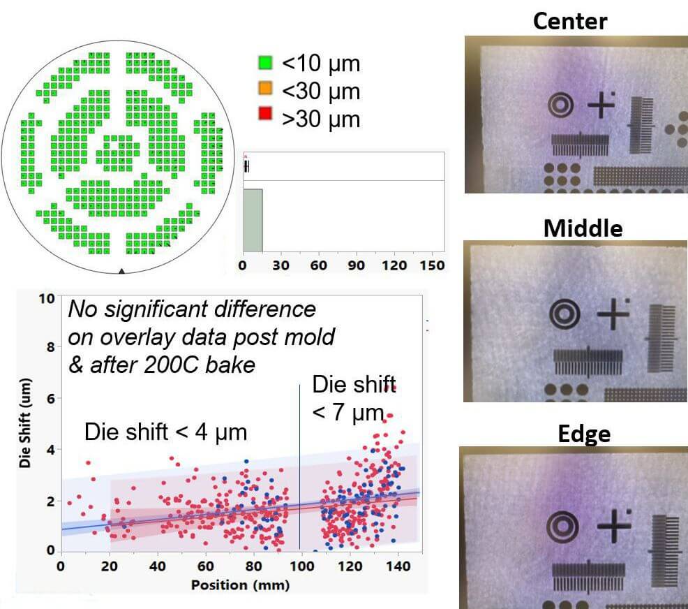
The team set up several experiments to evaluate different carrier systems, temporary adhesives, and mold materials. In partnership with Brewer Science Inc., a new temporary bonding material for room temperature die bonding was introduced, referred to as BrewerBOND® C1301. Both liquid and granular forms of advanced mold materials (referred to as M1 and M2) have been explored. The impact of these materials and processes on-die placement die shift and wafer geometry was investigated (Figure 3).
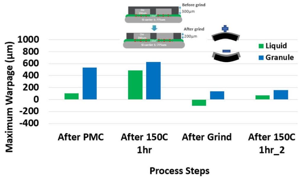
On blanket wafers, the granule mold material in combination with the temporary bonding material shows more stability than the liquid one when exposed to different temperatures. This can be explained by the higher glass transition temperature of granular vs. liquid mold materials.
On molded wafers with exposed embedded dies, the combination of a silicon carrier with the new temporary adhesive and advanced mold materials results in less than 2µm die-to-carrier mismatch, even after exposure to temperatures of 200°C for 2 hours — for both granular and liquid molds (Figure 4). Extremely low warpage of less than 200µm was achieved on the full 300mm wafer. These values are way below the ones reported in the literature.
The team also explored ways to efficiently de-bond the two carrier systems and remove the adhesive material. For the removal of carrier one, a mechanical de-bonding technique was used that did not affect the second bonding. The use of a mechanical-de-bondable silicon substrate was preferred, as it was compatible with the initial requirement of having alignment marks on the carrier substrate. For carrier two, a laser-assisted de-bonding was chosen for throughput and productivity reasons. Successful selective carrier de-bond has been demonstrated (Figure 5).
Conclusion
Warpage and die shift are two main challenges when processing molded substrates. The results presented in this study show that the combination of a new temporary bonding material with two different mold material types on a silicon substrate can address these challenges. A quasi-zero post-mold die shift and less than 200µm warpage could be demonstrated.
The new temporary carrier technology is a key enabler for imec’s flip-chip on FOWLP. But the importance of the results goes beyond that. First, the achievement of such very low warpage enables the processing of over-molded substrates in standard silicon equipment. Second, the results open a different avenue for the FOWLP processing approach in general. For example, fine-pitch redistribution layers in combination with chip-first approaches will now become possible.
Arnita Podpod graduated with a master’s degree in Materials Science and Engineering and with a bachelor’s degree in Applied Physics from the University of the Philippines. After graduation, she started at NXP Semiconductors as a Project (Materials) and Process Engineer and progressed to be a Senior Package Development Engineer with Fairchild Semiconductor Phils. Arnita joined imec in 2013 as a Senior R&D Engineer and is currently responsible for both Flip Chip on FOWLP projects and pre-assembly module integration within the imec 3D program.
Eric Beyne obtained a degree in electrical engineering in 1983 and the Ph.D. in Applied Sciences in 1990, both from the Katholieke Universiteit Leuven, Belgium. Since 1986 he has been with imec in Leuven, Belgium where he has worked on advanced packaging and interconnect technologies. Currently, he is imec Fellow and Program Director of imec’s 3D System Integration program. He received the European Semi Award 2016 for contributions to the development of 3D technologies.
This low-warpage temporary bonding and mold process for 3D die-to-wafer assembly was the recipient of the 2019 3DInCites Process of the Year Award.
This feature originally appeared in the 2020 Yearbook. Download your copy here.