
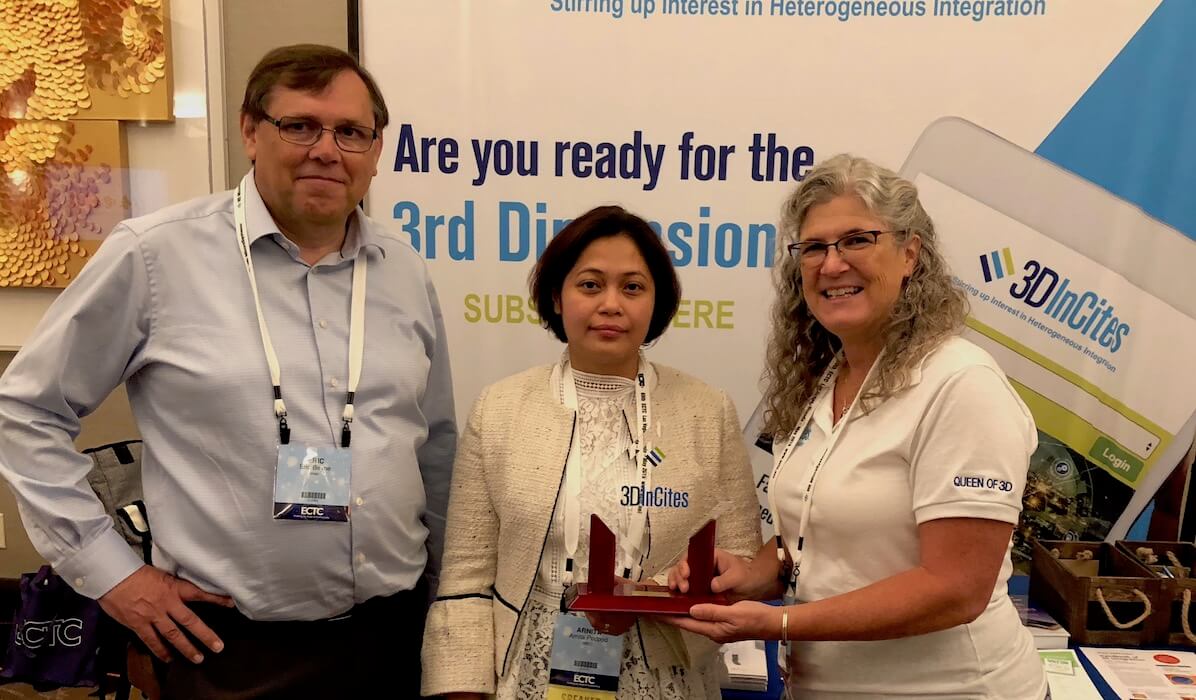
The recipient of the 2019 3D InCites Award for Process of the Year was Belgian research institute, imec, for its two-step wafer-level transfer mold process for 3D die-to-wafer assembly. The individual who nominated them for the award didn’t provide any more detail than that. But luckily at ECTC 2019, when I presented Eric Beyne with the award, he brought along Arnita Podpod, the research engineer responsible for the work that won the award. She sat down with me to explain the process, what challenges it addresses, and how it works.
Flip Chip on Fan-Out Wafer-Level Package
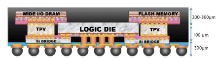
Podpod and her team were tasked with a project to demonstrate the new FOWLP concept: Flip Chip on Fan-Out Wafer Level Package (FC FOWP). An advanced temporary carrier technology is needed to enable this. What she came up with was a two-step wafer-level mold processes using compression mold technology. The concept package architecture targets a high-density, 3D flip-chip on fan-out wafer level package that integrates seven different chip components on both sides of the wafer including wide I/O DRAM, flash memory, logic, two high-density through package vias (TPVs), and two Si bridges comprising high-density fan-out with chip-to-TSV interconnect. The TPV and Si bridge connecting the wide I/O DRAM to logic with 20μm bump pitch are the key components to achieve ultra-high-density interconnect (Figure 1)
Podpod presented the initial work at the 2018 International Wafer-level Packaging Conference (IWLPC) focusing on assembly flow challenges and solutions for high-density fan-out build up. Ongoing work, presented at ECTC 2019, addresses die shift and warpage control. In October 2019 at IWLPC 2019, she will present advances in temporary carriers for high density fan-out build up.
The assembly process flow is described in Figure 2.

Materials were tested using dummy die so that critical steps could be addressed. Successful die placement was achieved on 300mm wafers at low temperatures. “Low temperature die placement is significant when you’re aiming for high-density interconnect, because the accurate placement is critical, and high temperatures can cause pattern recognition distortion during the die alignment and placement process,” explained Podpod. After accurate die placement, overlay data is captured before the overmolding step.
Podpod said that 5µm die placement accuracy is necessary to allow for 20µm bump pitch thermocompression bonding. Die shift and warpage happens after the molding step. The goal is to have a single adhesive that is compatible with two different mold compounds. Imec partnered with Brewer Science, testing adhesives with the two mold compounds to determine which would be most stable, and subsequently reduce die shift.
“But solving die shift is only the first part of the story,” explained Podpod. “The second part is enabling selective carrier debonding.”
Finding the Right Adhesives
There are two separate mold steps. One takes place on the first carrier after the silicon bridge is placed, after which the mold is ground to expose the pillars on the front side of the wafer. Then the thin stack is flipped onto the second carrier, and the first is removed so that memory die can be flip-chip attached. This is followed by wafer-level molding and subsequent removal of the second carrier.

For this, two experimental adhesives, also provided by Brewer, were tested. The goal was a good debond of carrier one after carrier two has been placed. “After removing the first carrier, the second carrier has to maintain warpage of less than 500µm,” explained Podpod. “The adhesive used to bond carrier two must be able to maintain the low warpage.”
The next challenge facing Podpod and her team is finding a way to debond carrier two without damaging the reconstructed wafer. They need to find a carrier two adhesive that will enable easy debonding of carrier one. It has to be a stronger adhesive than used for carrier one.
“We’ve identified set of materials that we think will work, but to be available for manufacturing, we need to prove the concept,” she said.
The ultimate goal is to provide a 3D FC fan-out package architecture for integrating logic and memory die. The concept is targeted to mobile and high-density applications, as well as high-performance computing.
These are just the basics of this very interesting process, as interpreted by me. Imec will publish a more technical article on 3D InCites telling the full story in the not-to-distant future, as it unfolds. ~ FvT


