As the semiconductor industry shifts focus from CMOS scaling to heterogeneous integration, the importance of surface preparation and wafer cleans during semiconductor device manufacturing is migrating from front-end wafer processing to back-end wafer level packaging processes. This, due to a combination of high-reliability applications, such as autonomous vehicles, 5G, artificial intelligence (AI), and the internet of things (IoT), and the high-density requirements of the advanced packaging technologies being used. For higher density fan-out wafer level packages (FOWLP), 2.5D and 3D integration technologies, proper preparation of the wafer surface, and ongoing clean steps throughout the process flow can greatly impact the reliability of the device that chip package is destined for. To get a clearer picture of how this impacts semiconductor equipment and materials suppliers, 3DInCites spoke with Anil Vijayendran, vice president of marketing at Veeco Instruments, Precision Surface Processing Division.
3D InCites: What do you see as the major trends in the advanced packaging space, especially in the context of surface preparation methods over the last 10 years?
Vijayendran: During this time the industry has seen a push toward wafer-level packaging (WLP) to meet growing performance demands (input/output [I/O] density, speed, form factor). Starting in 2009, the earliest form of fan-out wafer level packaging (FOWLP) was put into production. Now, more designs are being introduced by outsourced semiconductor assembly and test (OSAT) providers and foundries to address a growing application base.
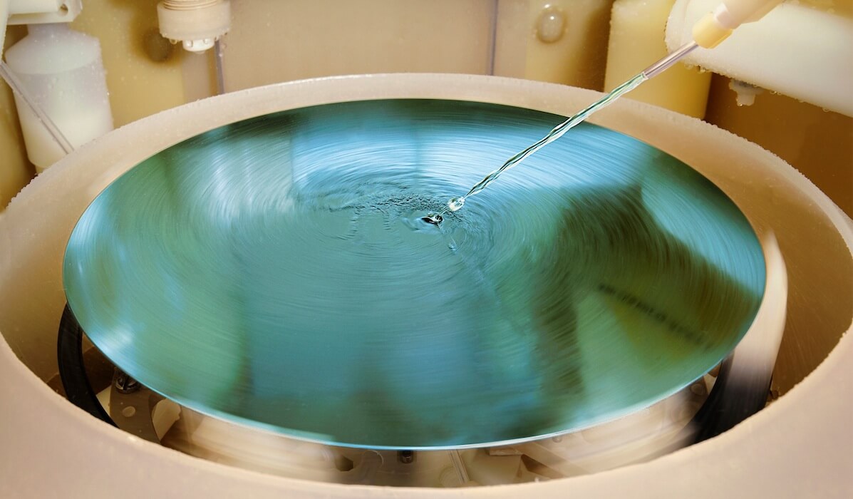
WLP requires a higher degree of control and process capability to maintain superior yields. From a surface preparation perspective, there are more cleaning steps with greater attention to defectivity. Specific to wet processing, the last 10 years has seen a greater number of strip, wet etch, and plating steps with a greater focus on dimensional control as this packaging method becomes more prevalent.
A key challenge to the adoption of WLP is cost. As such, suppliers have been tasked with working closely with fabs to meet the technical requirements of evolving packaging designs while still driving lower cost-of-ownership. This partnership is dependent on refined hardware, chemistry, and process to achieve sustainable high-volume manufacturing (HVM) results. Over the past decade, we have also seen an increased focus on environmental health and safety (EHS) by decreasing the adverse impacts of the chemical formulations used.
3D InCites: How have these trends affected the wet processing equipment and materials market?
Vijayendran: The equipment and materials industries have experienced significant change over the last 10 years. For example, manufacturers have relied heavily on wet benches for PR strip and etch processes. We’ve also seen the shift to single wafer equipment to improve process control. Wet benches, while less expensive, cannot meet the stringent uniformity and undercut requirements of advanced package techniques that single wafer equipment can. But, as mentioned before, these single wafer tools must deliver competitive CoO. This has led to a greater focus on filtration, reduced chemistry usage and chemical monitoring to minimize operational cost.
From a chemistry and materials view, the new advanced packaging methods have introduced new bumping and barrier materials – moving from traditional solder to materials such as gold, nickel, and titanium. Other shifts included transitioning from a fluxing process to a fluxless process as dimensions shrink in 2.5ED and 3D packaging applications. These changes required new chemistries and methods of delivery that maintain suitable throughput and are cost competitive. Moreover, chemistry manufacturers have invested significantly to optimize formulations that improve process characteristics such as material selectivity. From an EHS standpoint, there has also been a shift away from manually operated equipment and refinement in airflow design with wet process tools, thus reducing worker exposure by changing the tools performing the processes as opposed to changing the solvents themselves.
3D InCites: What challenges have packaging houses and equipment manufacturers and materials suppliers overcome in the last decade?
Vijayendran: A significant challenge for the industry has been to drive costs down while developing advanced technology that meets a wide range of application requirements. To overcome this hurdle, packaging players have consolidated. The trend towards fewer, but larger-sized, packaging entities allows for a greater amount of dedicated resources to focus on difficult technical problems. As these technical challenges became more complex, packaging houses continued to partner with equipment and material suppliers that can tailor solutions for their needs. This trend is especially prevalent today as larger equipment suppliers traditionally focused on front-end fabrication have receded from the advanced packaging market. Meanwhile, nimbler, mid-sized global companies and local suppliers have built product offerings dedicated to the advanced packaging market.
3D InCites: Looking forward, what technical challenges do new packaging techniques present to the wet processing market?
Vijayendran: As Moore’s Law slows, and the expense of device scaling below 7nm becomes increasingly challenging, chip manufacturers are looking to heterogeneous packaging techniques to achieve the performance benefit. Heterogeneous packaging involves significant complexity such as substrate and dimensional control, which impacts wet processes. The substrate material can be severely warped (in some cases up to 10mm), so the equipment must be able to handle this deflection while still maintaining process performance. The substrate type can also change from silicon to a glass or polymer compound. Equipment must be able to handle these different materials and in many cases on the same tool. From a dimensional standpoint, as the I/O count increases, the line/space (l/s) dimensions will shrink to 2µm while the number of redistribution (RDL) layers increases. Surface processes must be able to maintain dimensional control without damaging the substrate. As an example, for a 100µm bump, a 1µm undercut has a minimal effect on performance. At 2µm l/s, a 1µm undercut will be a performance killer. Equipment and chemistry manufacturers will be pushed to provide better process control to enable these smaller dimensions moving forward.

3D InCites: How about cost reduction trends and the impact on the industry past and present?
Vijayendran: In recent years, it has been a constant battle to maintain performance and low cost. Yet for these advanced packaging techniques to become mainstream, costs must continue to decrease. One way could be through implementation of panel-level packaging. By increasing the substrate size, manufacturers expand the usable die per substrate. On paper, this may seem like a simple concept, but it is more difficult in execution. Process performance on rectangular substrates will be different than on circular substrates. Wet processes, such as etch and clean, will not have the same uniformity on rectangular substrates as circular ones without re-thinking the equipment capability, process, and design. Difficulties with uniformity are further magnified by the sheer area of the panel as well as warpage across the panel. Handling such large substrates also poses significant challenges. Robotic systems and system architectures must be modified to handle the heavier substrate as well as the warpage. Lastly, moving all equipment suppliers to a new substrate size is of critical importance.
3D InCites: Given these challenges, what is your prediction for the wet processing equipment and materials market for the next few years?
Vijayendran: Looking ahead, we will see continued consolidation in the industry. Device manufacturers will push OSATs for more technical advances to enable further performance benefits to meet requirements for 5G, AI and the IoT. The industry will be focused on how to improve process control at 2µm l/s and below. Undercut control and defectivity will become more important as defects could now kill the package. Tools will become more flexible as the number of processes, wafer types, and sizes increase. Panel level packaging may also gain momentum for certain devices, which could be a catalyst for a parallel investment cycle in the industry. OSATs will need the flexibility to stay competitive and continue to push suppliers to offer more modular solutions. Finally, OSATs and foundries will need to partner with more global suppliers that have design and full process support capabilities as they look to build a competitive supply of advanced packaging offerings.
Editor’s note: This interview also appears in our print issue, 3D InCites: The First Decade. Download the complete issue here.