
Data is now the world’s most valuable resource.
Solid-state storage of data is driving an innovation revolution built upon 50 years of progress.
Here we look at the dual-gate thin film transistor (DG-TFT), an extremely versatile solid-state data storage device that can be used in monolithic 3D as either a flash memory or a dynamic memory element. It has the potential to provide a path not only to higher capacity and lower cost 3D flash, but also to take DRAM into the third dimension.
Figure 1 shows the basic DG-TFT. It is a four-terminal device containing two field effect transistors. The two gates can be independently driven. Each field effect device provides independent access between source and drain.
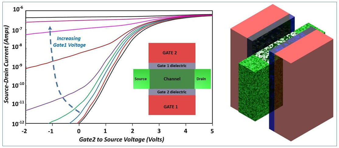
Memory capability is provided by using charge trapping in sandwich layers of silicon nitride and silicon oxide materials used as gate dielectrics. These can be used in either field effect device or both.
The effect of charge storage on the conductivity of the two devices is shown in Figure 2. The charge storage has a large effect on the field effect transistor where the storage takes place while a minimal but non-zero effect on the other transistor. This means that data can be stored independently in each device or in both with minimal interaction between the two. In addition, reading data must use the gate adjacent to the stored charge being read.
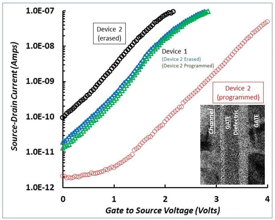
The use of the DG-TFT as a 3D flash element for storage-class memory has been explained previously. What is new is its potential use as a 3D dynamic memory.

In a DRAM, data is stored as charge on a capacitor and kept there by a field effect transistor in the off state. Since charge leaks away from the capacitor, refreshing has to restore its level every few tens of milliseconds. This dissipates power. The lateral shrinking of DRAM is fast approaching limitations but 3D stacking of the existing approach looks to be a stretch.
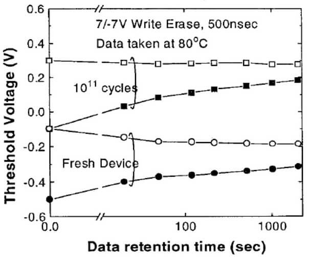
Instead of storing charge on conducting plates of a capacitor, we can use the traps in the dielectric sandwich of a field effect transistor. The difference with charge trap Flash is that the sandwich layers are thinner resulting in orders of magnitude increased endurance and lower program and erase voltages. The tradeoff is with retention but this is still orders of magnitude better than DRAM.
Figure 3 shows retention measured after 100 billion program/erase cycles on a crystalline field effect transistor with thin charge trapping sandwich layers reported by UC Berkeley in 1995.
The application of this approach to the DG-TFT provides a path to ultra-high density 3D dynamic memory with low-power dissipation.
In summary, the DG-TFT is a very versatile solid state data storage device that can be stacked in 3D to provide paths to ultra-high density, low-cost flash and dynamic memory.