
About 50 years ago, I started my career as a system-level designer, focused on an interface card for the Siemens T 1000. It was the first electronic teletype, destined to ship in extremely high volumes all over the world. When Siemens ramped up production, they invited me to the factory and showed me a big train car, packed up to the ceiling with my small PCB designs. Then I finally understood why my manager had pounded me almost daily with “You must reduce component and assembly cost!” This “train car impression” always encourages me to push for higher levels of integration, e.g. 2.5/3D-ICs, because they are, in my opinion, our most promising way to reduce component and assembly cost for electronic systems.
The Interface Between Memory and Processors
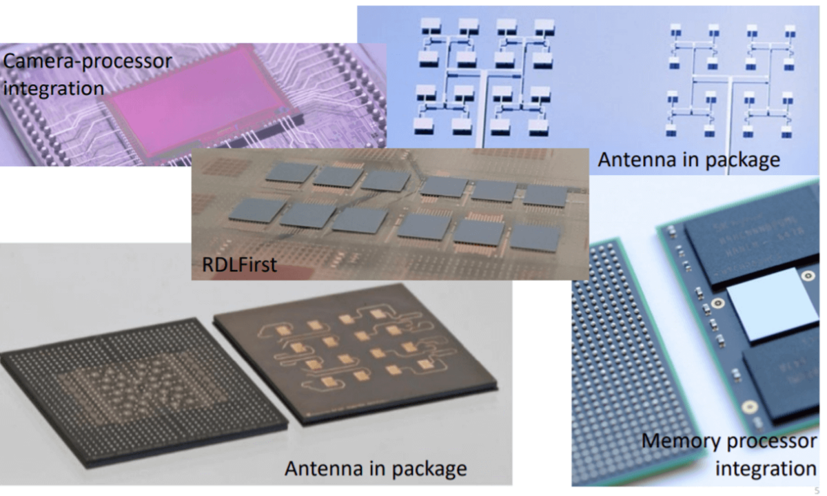
At the iMAPS webinar on July 1, Andy Heinig, Department Head for Efficient Electronics at the Fraunhofer Institute for Integrated Circuits (IIS) in Dresden presented a very telling example for designing cost-effective electronic systems. He showed how to increase bandwidth and power efficiency of interfaces between processors and memory – to tear down the dreaded Memory Wall. Heinig started with several slides about recent accomplishments at Fraunhofer IIS, then described Germany’s large Fraunhofer Gesellschaft, founded in 1949. Today its 74 institutes, including ISS, employ 28,000 people, the majority of them qualified scientists and engineers. See examples for some of IIS’ latest integration projects in the image above.
More Moore (Chiplets) AND More than Moore (Advanced Packaging)
50+ years of following Moore’s Law has demonstrated that higher levels of integration increase performance per Watt and allow us to pack more and more – primarily digital – functionality into a single-die IC. However, continued shrinking of feature sizes has not only increased the technical integration challenges, like development time, risk, and cost, but also the cost per transistor, and with it, has raised the cost per function.
In addition, when customers need heterogeneous functions (logic, memories, analog, RF, SERDES, MEMS, …) packed into a single-die ICs, technical capabilities and economics fail. That’s why customers are demanding that suppliers pack multiple dice (a.k.a. chiplets), all manufactured in their most suitable process technology, into an IC package. In the latest decade, multi-die IC packaging technologies have matured significantly and a growing number of system and IC designers are now relying on multi-die ICs in advanced packages, to meet specifications as well as schedules and cost targets. With multiple dice in a package, power and heat management, signal and power integrity as well as die to die interconnects are becoming more challenging. Currently, the most common way of interconnecting multiple dice is using a silicon, organic, or glass interposer (2.5D-ICs).
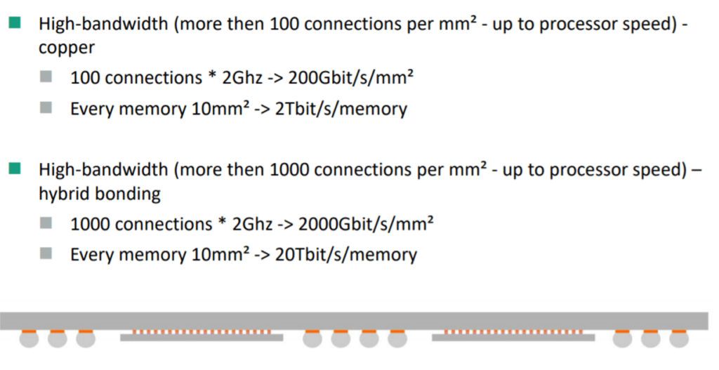
Heinig discussed in his presentation an example for further increasing both bandwidth and power-efficiency – while eliminating the cost of interposers to interconnect chiplets or using TSVs as signal or power paths to the PCB. Figure 2 shows Heinig’s 3D-IC stack-up.
Tearing Down the dreaded Memory Wall, Demonstrated with Numbers
In addition to the the cross-section of a flexible and scalable system build-up with face-to-face, vertically stacked dice, Figure 2 shows several calculations. They assume that the large processor die interfaces directly with the attached memory dice, in the first example, via copper studs and pads. They enable 100 connections per square millimeter. At a data rate of 2 Gbits/sec x 100 connections/mm2 x 10 mm2 interconnect area on every memory die, 2 Tbits/sec of bandwidth between the large logic die and a memory can be achieved. Figure 2 also shows in the second example that hybrid bonding, assuming a very conservative interconnect density of only 1000 connections per mm2, already increases the bandwidth to 20 Tbits/sec per memory die (assuming again 10 mm2 interconnect area).
Design tools and package assembly design kit(s) enable lower development cost/time/risk and lower unit cost.
As market pressure grows to further increase the level of integration and meet tighter schedules, achieving the demanded results with traditional prototyping becomes practically impossible. Like in the early days of ASIC technology, electronic design automation (EDA) tools are coming to the rescue. Fed with accurate data, contained in a package assembly design kit (P-ADK), like materials characteristics, package design rules, models of building blocks (a.k.a. chiplets), the EDA tools can minimize the time needed for iterations within every design step and help to optimize the die-package-board interactions.
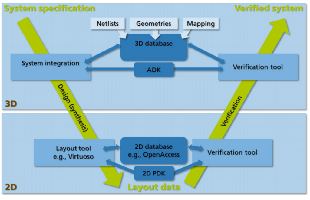
EDA tools also allow designers to quickly make power/performance/cost trade-offs and enable them to simulate and consider the impact of materials variations as well as manufacturing tolerances on a design’s manufacturing yield, to significantly improve it. Best of all, EDA tools can exhaustively verify functionality, timing, power dissipation and reliability of a design much faster and more accurately than a series of split-lots and/or prototypes would be able to. The block diagram of Heinig’s design and verification flow, Figure 3, shows the most important inputs needed and key design steps.
Final Assembly on a Printed Circuit Evaluation Board
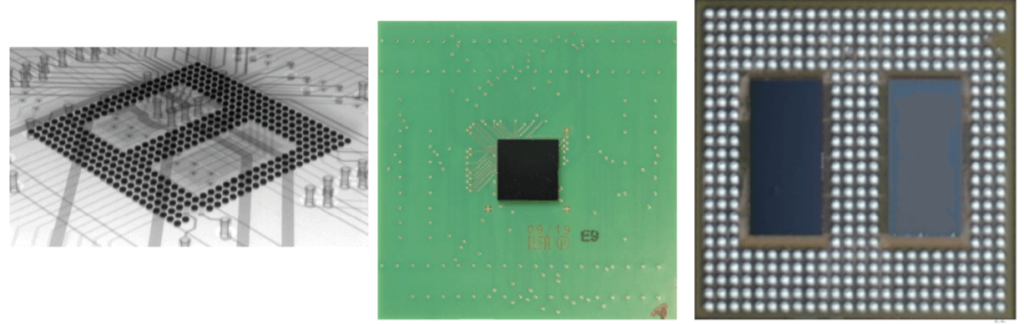
In addition to discussing the multi-die IC design, Heinig also described the validation board used in this project. Figure 4 shows an X-ray view of the multi-die design (left) a top-down view of the board (center) and a bottom view of the 3D-IC with the two memories attached (right).
Personal Comments
Stacking logic and memory vertically (like in this design) offers the best possible bandwidth. However, for high-performance and high-power applications, the much higher operating temperature of a logic die will force a DRAM die to refresh itself frequently, reducing access time (and bandwidth) significantly. For high power and high-performance applications, the 2.5D architectures are better suited.

Heinig’s design example conveys another important benefit of 3D stacking – the significant reduction of power dissipation, due to much shorter interconnect lengths and smaller capacitances. Especially battery-power applications appreciate this benefit, that’s why the versatility and scalability of Heinig’s example architecture is a great reference for using multi-die ICs to extend battery life of handheld devices, IoT edge nodes, and other applications.
During my 40+ years in the semiconductor industry, I have introduced many new technologies and have observed every time pretty much the same behavior of the supply chain, early adopters, and mainstream users. Knowing that “history repeats itself”- here is a list of key steps and capabilities that have made and still make ASIC technology successful:
- High-level design planning tools help to find the best architecture for the application at hand.
- EDA design tools enable ASIC developers to manage larger and larger transistor counts, higher speeds and lower unit cost.
- Extensive user training, e.g. educating 1000 power users/influencers created a dominant market position for an EDA tool.
- Accurate wafer-foundry PDKs give die-developers exact guidance and tell them what’s possible and what’s not allowed.
- Building blocks, like embedded memories, processors, data converters, etc. increase ASIC designers’ productivity.
- Sign-off quality verification flows and clear hand-off criteria assure that a design is manufacturable and yields very well.
- Design and manufacturing standards enable world-wide cooperation, higher efficiency, and lower cost.
Translating the proven ASIC success criteria into the Advanced Packaging ecosystem, I want to point out:
- “Path-finding” tools will enable multi-die designers to evaluate architectures, then implement the most suitable one.
- EDA design tools can simplify multi-die design, enable die-package-board tradeoffs, and make large designs manageable.
- P-ADKs will give die and package designers guidance on how to best utilize assembly partners’ capabilities – at the lowest cost.
- Education/user training, e.g. the heterogeneous integration roadmap efforts accelerate and broaden market acceptance
- A broad range of chiplets will improve 2.5/3D-IC designers’ productivity, improve time to profit, and system reliability.
- Sign-off quality verification flows and clear hand-off criteria will minimize iterations, save time, and engineering costs.
- Standards across the entire supply chain will increase profitability at all steps, will accelerate market acceptance for technology innovations, and reduce time to market for every multi-die design.
Please use some of these points to discuss with your design and manufacturing partner(s) how your next (or first) integration project can best take advantage of every partner’s capabilities and contribute to your success.
On the iMAPS website, you can get all the slides Heinig used, request an MP4 file of his entire presentation, review previous presentations in this series, and register for upcoming virtual events, e.g. Laura Mirkarimi’s presentation about Xperi’s Hybrid Bonding technology.
~ Herb


