
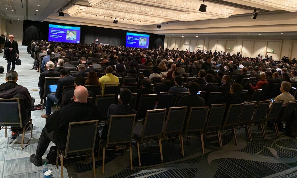
The San Francisco Hilton on O’Farrell Street welcomed IEDM 2019 and it’s 1800 attendees in early December. While the conference name implies its focus to be the International Electronic DEVICES Meeting, I was glad to see that IEDM looked again way beyond devices into application-specific topics and system-level challenges of electronic systems.
I also was happy to see that the average age of the attendees is getting younger. Many dark-haired male and female engineers, especially from Asia, attended and demonstrated that they’ll continue to advance the electronic systems industry beyond what my generation has been able to accomplish in the last 50 years.
Nine parallel tracks offered in-depth information about hot topics like extreme ultraviolet (EUV) lithography advancements, new transistor architectures, new memory technologies, new materials, advanced single and multi-die packaging, lots of MEMS and sensors information as well as artificial intelligence (AI) topics and how to improve reliability on the component and system level. The presenters’ messages, as well as the questions from the audience, conveyed energy, optimism, and hope that the weakness our industry has endured in 2019 will not continue into 2020 and beyond.
The Short Courses
For me, IEDM started on Sunday morning with a series of presentations about memory-centric computing. Experts from Micron, Samsung, Intel, Facebook, Georgia Tech, and Western Digital described the benefits and trade-offs that new memory technologies offer and explained how they impact compute performance and power efficiency of electronic systems. Allow me to highlight what is useful for 3D InCites readers.
Samsung’s Kyomin Sohn showed a comparison between using twelve GDDR5 memories, 1GB each, versus using four, second generation, high bandwidth memory (HBM2s) with 4GB each:
- Total memory size: Twelve GDDR5 ICs offer 12GBytes, four HBM2s offer 16GB today
- Board space needed for processor and memories: 3120 versus 792mm2
- Power dissipation: 18.3 versus 9.1W
- Total number of connections times signaling speed equals available bandwidth between processor and memory: 384 x 8Gbps = 384GB/sec versus 4096 x 2Gbps = 1024GB/sec.
In summary: Four HBM2s with “only” 4GB each offer 33% more memory, consume one-quarter of the board space, only half as much power and almost three times higher bandwidth, compared to 12 GDDR5 ICs.
Later in his presentation, Sohn announced Samsung’s plans for increasing the signaling speed from currently 2 to 2.8 then 3.6Gbps for HBM2s. For the HBM3 generation, Samsung targets up to 4 Gbps. The company will also expand the memory capacity from the 4GB used in the example above to 8, then will offer 16, 24, and even plan to reach 32 GB per HBM by increasing every memory layer from 1 to 2 GB and the number of layers from four up to sixteen.
In my opinion, electronic systems architects, processor designers as well as assembly and test experts need to become familiar with how to best utilize the power of these memory sub-systems and learn how to test them exhaustively – as components and within the system context. Only then can the supply chain assure system reliability as well as justify the HBMs higher cost per bit, compared to other high-speed memory ICs.
From the Keynotes
After the traditional awards presentations, executives from Intel, ASML, and Kioxia Corporation (formerly Toshiba Memory) conveyed a very upbeat message for our industry. Robert Chau, Sr Fellow at Intel, started his presentation with “The Future of Moore’s Law is Bright!”, then explained that scaling of gate pitches, cell heights, and contact sizes can continue. Among other innovations, gate-all-around (GAA), nanowire/sheet transistors, graphene layers, germanium for PMOS transistors, gallium nitride, Intel’s production-ready STT-MRAMs, ferroelectric eDRAMs, and other technologies will drive our industry forward.
Chau also pointed out that direct self-assembly (DSA) will complement the progress EUV lithography is making to enable smaller feature sizes. He also praised advanced IC packaging technologies for driving system scaling.
I think it is great to see Intel utilizing its powerful IC packaging team to further extend Moore’s Law. Chau also highlighted Intel’s omnidirectional interconnects and encouraged the audience to attend Intel’s Lakefield presentation in session 19.6. to learn about this hybrid CPU. (More about this topic later in this blog)
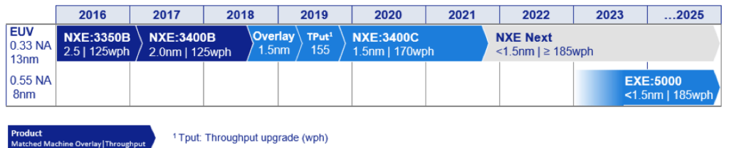
Martin van den Brink, President, and CTO, ASML, emphasized that performance and cost drive high-performance computing. He proudly confirmed that ASML’s progress in EUV lithography, new metrology tools, and advanced computing algorithms have made their technology capable and cost-effective for high volume production (Figure 1). Brink also mentioned that EDA partners and photo-resist suppliers were essential for this success.

Ishimaru, from the Institute of Memory Technology R&D at Kioxia Corporation, also conveyed a lot of optimism about the semiconductor industry’s future. He projected that by 2030 the 3D NANDs will use ~1000 layers and achieve ten times higher speeds (= 25Gbps) than today, by using PAM-4.
Technology and Electronic Systems Applications
Session 10 focused on human-machine interfaces (HMI) using wearables, humanoid robots, AR/VR glasses, and other means to monitor humans and enable them to control machinery. Researchers from imec, EPFL, Keio University, Tokyo University, and Tyndall, as well as Facebook and Samsung, outlined their work towards user-friendly HMIs that work reliably both ways. Here are two examples of their long-range research activities:
Professor Ohnishi from Keio University explained the importance of haptic (by touch) communication. While haptics is not that important for most industrial robots, for service robots it’s very important that they can “feel” what they are touching and how much pressure they exert. It also allows them to control the speed at which they move and provide feedback to their operator as needed. This feedback loop is also essential for a robot to perform routine tasks autonomously.
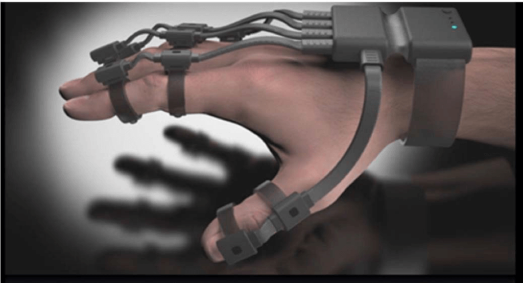
Brendan O’Flynn from Tyndall National Institute explained how its battery-operated haptic glove (Figure 2) communicates wirelessly and bi-directionally, with very low latency, with a robot that may operate in a hazardous environment. This glove-based system can be combined with AR/VR glasses and enables the operator and the robot to perform complex tasks accurately while protecting the operator.
In session 16, four people from Sony, as well as speakers from OmniVision, Samsung, and STMicro presented the important features and benefits of optical sensors to a very engaged audience, in a fully packed room. We learned how these companies have achieved pixel sizes of less than one micron, and why they use back-illuminated CMOS image sensors (BI-CIS). They explained trade-offs between global and rolling shutter, how to accomplish high dynamic range (HDR), and how phase-detect autofocus (PDAF), on-chip lenses (OCL) and on-chip color filters (OCCFs) work. Together with other advancements in digital photography, these experts help to make the tiny built-in cameras that are such important differentiators for smartphones.
Advanced Logic Technology
ARM’s Divya Prasad explained how buried power rails and backside power grids reduce voltage drop and free up front-side area to pack more functionality on a die.
Doug Ingerly presented Intel’s new, omnidirectional interconnect technology that combines EMIB and Foveros to interconnect a 22 nm base die with a 10 nm CPU and two layers of DRAM to build this hybrid CPU, called Lakefield. (See Video).
Figure 3: Intel’s Lakefield Hybrid CPU
In Summary
IEDM2019 has clearly conveyed that the semiconductor industry is on its way to making major changes in response to new and emerging market needs: multi-die ICs meet the need for integrating heterogeneous functions cost-effectively, improved CMOS image sensors differentiate smartphones, MEMS and sensors connect the real world – which is analog and multi-physics – with ever-increasing digital compute power and new materials that allow higher frequencies and operating temperatures. AI algorithms and ever faster computing will make the electronic systems serving us smarter, safer and more reliable. Thanks for reading ~ Herb


