
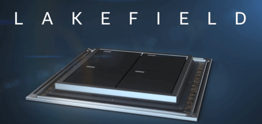
At CES 2019, Intel previewed a new client platform, code-named “Lakefield”. It featured the first iteration of its new innovative Foveros 3D packaging technology. The Lakefield stacked module will contain:
- 10nm hybrid CPU architecture
- Gen 11 graphics
- Multiple dies stacked on top of each other
The die is then stacked using micro-bumps on the active interposer through which through silicon vias (TSVs) are drilled to connect with solder bumps and eventually the final package. This hybrid CPU architecture makes it possible to combine different pieces of IP, which might have previously been discrete, into a single module with a smaller motherboard footprint. This results in a thinner and lighter form factor. The module is just 12×12mm. Intel reports that Lakefield will be in production this year.
The Lakefield that Intel previewed consists of least four layers. DRAM layers are placed on top of the compute chiplet layer that contains the 10nm CPU and GPU and then placed on top of the base layer containing cache and I/O (Figure 2).
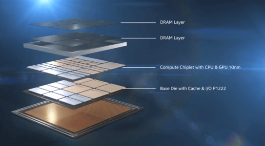
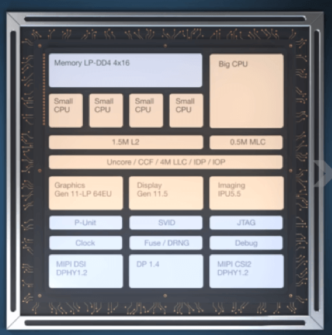
The top two layers are composed of the DRAM to supplement the processor memory. The 3rd layer is the compute chiplet layer with a hybrid CPU architecture and graphics based on the 10nm process node. The hybrid CPU architecture has a total of five individual cores. There are also four small CPUs that are based on the 10nm process that is optimized for power efficiency (Figure 3)
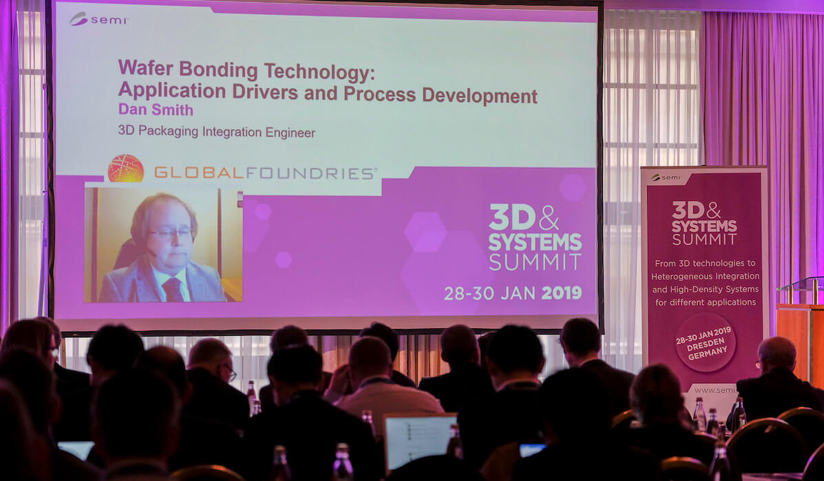
SEMI Europe 3D and Systems Summit – Dresden
The SEMI Europe 3D and Systems Summit was held in Dresden in January. Over the next few blogs, we will take a look at some of the more interesting presentations at that conference.

Global Foundries (GF)
Dan Smith of GF discussed wafer bonding technologies. When we normally think of stacking layers we think of micro bumps which, at the leading edge, are down to a pitch of 30-40µm. But we also are aware that many years ago, Ziptronix (first acquired by Invensas and now part of Xperi) detailed and patented what they called DBI™(direct bond interconnect) which was/is capable of 1-2µm pitch interconnection.With DBI technology, the under bump metallization (UBM), underfill and micro-bumps are replaced with a DBI metallization layer. Bonding at die or wafer level is initiated at room temperature followed by a batch anneal at low temperature. Sony Introduced the DBI technology in the Samsung Galaxy S7.The packaging group at CEA Leti has also been active in this technology area.
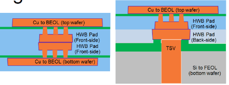
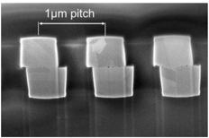
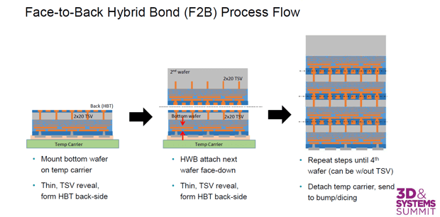
Figure 4 shows a Leti connection on a 1µm pitch which they call direct hybrid bonding. The latter name…i.e hybrid wafer bonding, or simply, hybrid bonding, is the name that has caught on in the industry.GF has now announced that they are developing hybrid bonding technology in their 12LP technology for both face-to-face (F2F) and front-to-back (F2B) stacking. Mechanical and electrical studies are currently underway with final qualification expected in the second half of 2019. Front side connections are formed on the last Cu layer of BEOL and the back side connections are formed to the bottom of the TSV (FIgure 5). Wafer bow between the two wafers can cause alignment issues, but the bonding tool has “shape correction” on the chucks to mitigate the issue. So far they have achieved F2F sub 5um pitch hybrid bonding with 5 x 50um TSV on a 150um pitch. The F2F and F2B hybrid bonding process flows are shown below. 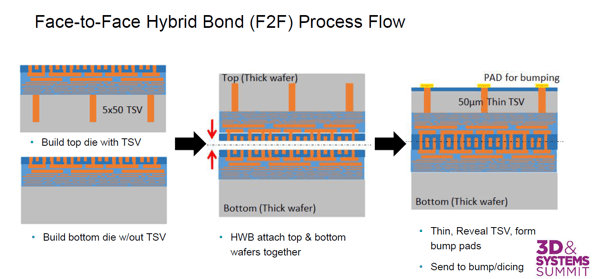
 It will be of significant interest to see if such hybrid bonding can achieve adoption beyond CMOS image sensor production. For all the latest in advanced packaging stay linked to IFTLE…………………….


