
Building on their previous announcements of its embedded interconnect bridge, EMIB, ( see IFTLE 324 “Intel EMIB Implementation in the Stratix MX”) and Foveros technologies (see IFTLE 400 “Intel Logic-Logic 3DIC and Chiplets are Finally Here”), Intel, as a prequel to SEMICON West this year, hosted a media/analyst event to provide details on its three new enabling technologies for advanced packaging: Co-EMIB (using EMIB and Foveros together), managed data input/output (MDIO) and Omni-directional interconnect (ODI). They also included details about a hybrid bonding technology similar to that developed by Ziptronix and a proprietary tester that predicts Known Good Die (KGD) by simulating conditions that they would experience in the final package.
A news release from the company states: “Packaging is becoming a catalyst for product innovation”….. allow(ing) for the integration of diverse computing engines across multiple process technologies with performance parameters similar to a single die, but with a platform scope that far exceeds the die-size limit of single-die integration. These technologies will improve product-level performance, power, and area while enabling a complete rethinking of the system architecture.”
“We are in the heterogeneous integration game now,” explained Babek Sabi, VP of assembly and test, Intel, “It’s not just about Moore’s Law anymore. Our vision is to develop leading technology to connect chips and chiplets in a package to match the functionality of a monolithic system-on-chip. A heterogeneous approach gives our chip architects unprecedented flexibility to mix and match IP blocks and process technologies with various memory and I/O elements in new device form factors. Intel’s vertically integrated structure provides an advantage in the era of heterogeneous integration, giving us an unmatched ability to co-optimize architecture, process, and packaging to deliver leadership products.” He called it the IDM Advantage.
Co-EMIB: An Enabling Technology for Interconnecting Foveros
Intel’s EMIB and Foveros technologies leverage high-density interconnects for high bandwidth at low power, with I/O density on par with or better than competitive approaches. EMIB offers localized interconnect advantages that aren’t possible with Si interposers. Foveros can be described as a Si interposer using active silicon. Depending on how chips are partitioned architecturally, there are reasons to use both.
By blending both EMIB and Foveros, Intel says it has found a way to blend 2D and 3D together, providing a transition from solder-based interconnects to non-solder-based interconnects (Figure 1).
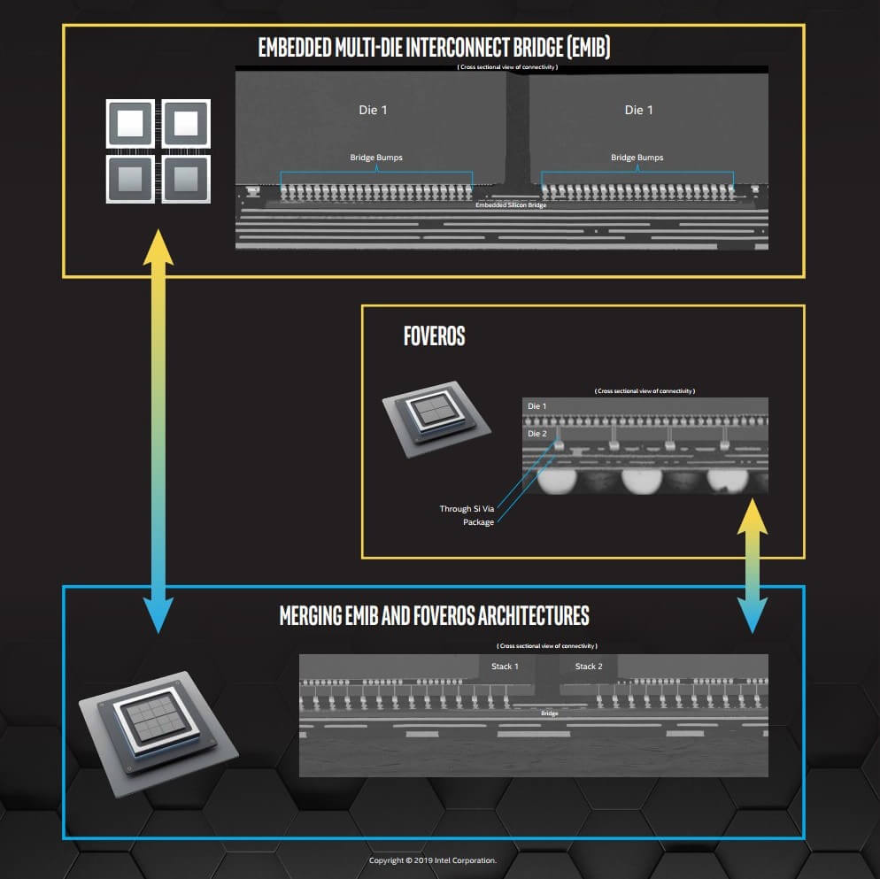
The company’s new Co-EMIB technology links even more computing performance and capability together. It allows for the interconnection of two or more Foveros elements with essentially the performance of a single chip. Designers can also connect analog, memory and other tiles with very high bandwidth and at very low power using Co-EMIB.
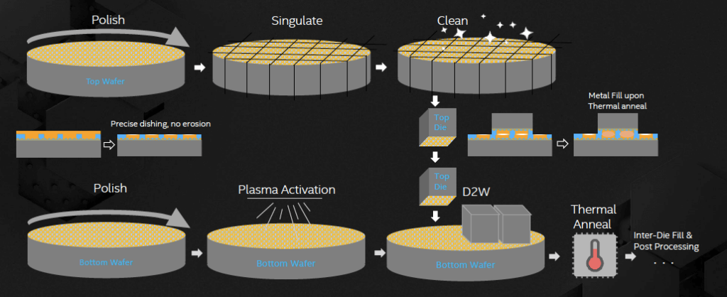
While traditionally interconnects are formed using thermocompression bonding and solder, Johanna Swan, Intel Fellow, explained that the research team is developing a die-to-wafer hybrid bonding approach to enable high-density interconnects for Co-EMIB. This approach uses thermal anneal to create covalent bonds. When asked if this was the DBI Ultra approach, Swan commented: “Its generic term is hybrid bonding. DBI is one company’s product. This is a similar technology.”(Figure 2)
Omni-directional Interconnect
ODI is basically a 70mm thick vertical link for delivering power to a top die from a substrate. The top chip can communicate laterally with other chiplets through lithographically defined vias, where via width is equal to trace width. Swan called these zero misaligned vias (ZMV). It can also communicate vertically with through-silicon vias (TSVs) in the base die below, similar to Foveros. Larger than traditional TSVs, the large vias provide lower resistance power delivery along with higher bandwidth and lower latency. This approach also reduces the number of TSVs required in the base die.
Manage Data Input/Output
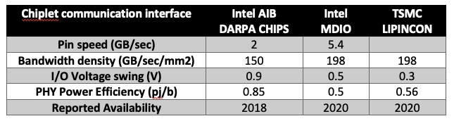
MDIO IP core is a two-wire standard management interface that implements a standardized method to access the external Ethernet PHY device management registers for configuration and management purposes. MDIO is the next-generation of Intel’s AIB physical interface for connecting chiplets. Those of you following the progress of the DARPA CHIPS project on IFTLE know all about the use of the Intel AIB interface. The technology enables a modular approach to system design with a library of chiplet intellectual property blocks. MDIO reportedly provides better power efficiency and more than double the pin speed and bandwidth density offered by AIB.
MDIO Intel claims MDIO is on par with LIPINCON technology, which TSMC recently announced. LIPINCON is an interconnect architecture designed for chiplet designs with advanced packaging technologies such as InFO and CoWoS. Both TSMC and Intel report that they will begin using these interfaces in 2020 (Table 1)

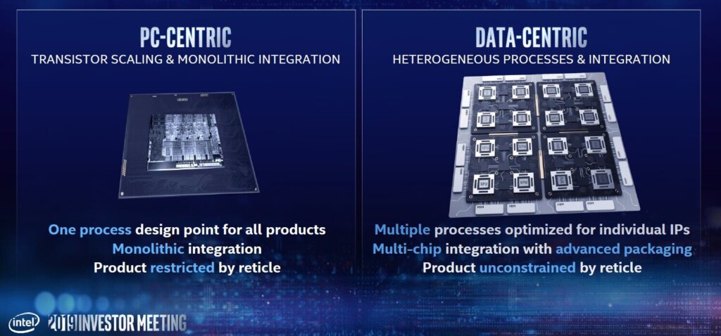
At the recent Intel investors meeting, the company announced that advanced packaging was helping change this from a PC centric to a data-centric world as shown in Figure 3.
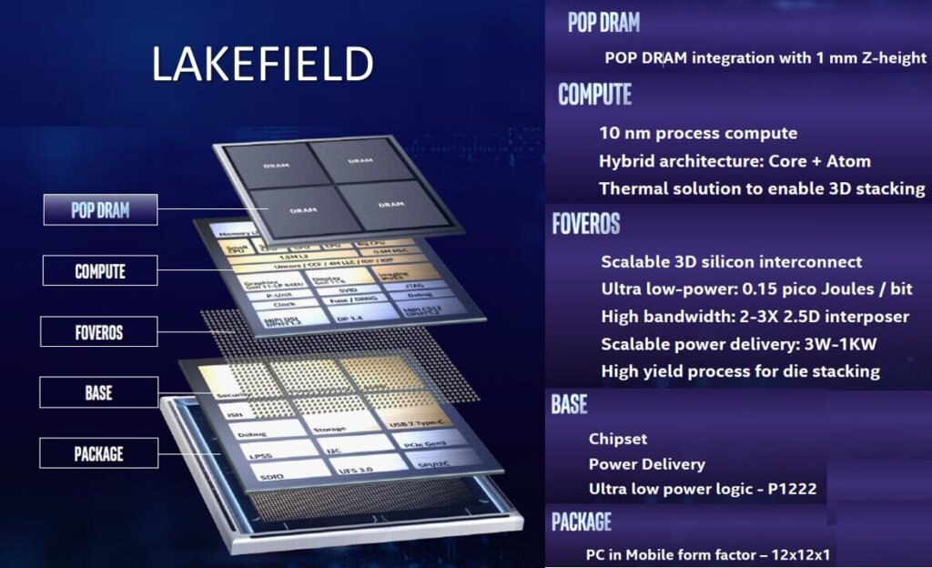
The use of technologies like Foveros will reportedly be released in 2019 in the Intel Lakefield processor which will use chiplets, Foveros, and Intel’s “long-awaited” 10nm technology.
To lift a phrase out of the “urban dictionary”…advanced packaging “That’s where it’s at!”
For all the latest in Advanced Packaging stay linked to IFTLE………………..


