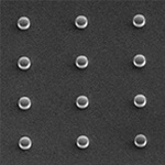
 SSEC’s wet TSV reveal process achieves -/+ 0.7% Si thickness uniformity under the appropriate post grinding conditions with fast throughput. The two-step process starts with a spin etch for a smooth, fast etch at 10µm/min. The etch is stopped 2µm above the TSVs and then finishes with a selective etch process (Si:SiO2 >2,500) to endpoint on the TSV based on Si thickness measurements done on the SSEC’s platform.
Testimonial
Via reveal is a critical process step in 2.5D and 3D IC technologies that involves thinning the backside of the wafer to reveal the copper interconnects, and is a focus area to improve process control and reduce costs. The improved two-step process uses an hydrofluoric and nitric acid mixture as the smoothing etch chemistry, and Sachem’s RevealEtch chemistry for the selective etch step. This process eliminates the need for CMP or dry polish. Neither TMAH nor KOH is used, eliminating health concerns and extensive cleaning requirements.
Performed on SSEC’s WaferEtch™ platform, which features integrated metrology for performing thickness measurement and end point detection, this wet etch TSV reveal process replaces four tools required for dry etch process including: CMP, plasma etch, clean, and silicon thickness measurement. The CoO is estimated to be 68% less than dry approaches, Lower development and production costs helps bring 3D ICs to high volume manufacturing.
- SSEC Website
- Date this Product was Introduced to the market: 7/8/2013
- Category Product is being Nominated for: P3D
- Technical Information for Wet Etch Process for TSV Reveal


