
While Herb Reiter dove deep into the technology sessions at ECTC 2015, I spent most of my time picking the brains of suppliers who have introduced products targeting advanced wafer level packaging and 3D ICs. Overall, I’ve noticed efforts are becoming really targeted, and are focused on remaining challenges like thermal management, improving yields, and increasing throughput, addressing assembly challenges, and of course, optimizing processes to bring down the cost of 3D ICs.
First off, I checked in with Andrew Ho, Dow Corning, for an update on the thermal interface material developed in collaboration with IBM, that Dow Corning first presented in concept at ECTC 2014.
The more functionality a chip has in it, the more heat it generates, explained Ho. Thermal management has become a bottleneck for both 2D and 3D integration schemes. Originally developed for flip chip applications (and presented again this year in the flip chip session), TC3040 is a silicone based, gel form adhesive that serves as both a lid sealant and thermal interface material used to drive the heat away from the chip inside the package, explained Ho. Ho says it also can provide a solution for getting the heat out of 3D stacked chips by driving the heat from the top die to the connected lid.
The big news this year for TC3040 is that Dow Corning now has validation from its partners, and the material will be implemented in high end computing applications.
A good sign that 3D ICs are nearer to high volume production is that equipment suppliers who cater to volume manufacturing are seeing opportunity in advanced wafer level packaging and 3D, and are jumping into the mix. We saw it early on with Applied Materials, and now Lam Research and KLAT Tencor have introduced offerings targeting wafer level and 3D IC processes.
Lam Research has now joined Veeco Precision Surface Processing (formerly SSEC) as promoters of wet etch processes for TSV reveal as a significantly lower cost option to plasma etch. In his presentation, Stefan Detterbeck, Lam Research, presented an acidic wet etch process combining spin etch with 5% Tetramethylammonium hydroxide (TMAH) to achieve optimized uniformity in the TSV reveal step.
Having another equipment manufacturer in the wet etch game is a great endorsement of the process. What both companies are up against is established DRIE tools in the field that are already being used for the TSV reveal step. However, since the OSATS aren’t putting in the TSVs and dealing only with the backside processing, a low cost wet option may be attractive to them. What Lam is up against is the fact that its process is TMAH-based. TMAH a caustic chemistry that has major health issues, is highly corrosive, and crosses the skin barrier.
At ECTC 2014, Veeco Precision Surface Processing (formerly SSEC), along with chemistry partner, Sachem, presented results of wet etch using chemistry that is neither TMAH-based or its current alternative, potassium hydrochloride (KOH), which has residue and cleaning issues. This chemistry, commercialized by Sachem as RevealEtch, was developed specifically for the reveal step, and according to last year’s presentation, etches silicon with high precision and a lack of roughness, without the health issues of TMAH. If Lam tests its processes on the multi-nozzle tool referenced in the presentation using RevealEtch instead of TMAH, then they might be on to something.
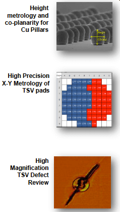 KLA Tencor’s big news at this year’s ECTC was the launch of its CIRCL-AP platform for all surface wafer inspection and metrology for advanced wafer level packaging (AWLP) and 3D IC in high volume manufacturing (HVM). According to Sumant Sood, KLA Tencor, the platform comprises 3 main modules: the 8-series for frontside inspection and metrology, the CV350i for edge inspection and metrology, and the Micro300 metrology for 2D and 3D metrology. Sood noted that the Micro300 is the most critical to 3D integration for process control (Figure 1). “TSV processing means lots of 3D features. We need to measure the height and diameter of those features and this is the right module for that,” he said.

So my question; what makes this system different from what’s available on the market today? It’s totally integrated, explained Sood. While other systems offer similar metrology and inspection processes, they aren’t totally integrated into one system that is completely automated, rather than relying on FOUP handling. Additionally, Sood pointed out that lots of 3D IC and packaging wafers are very warped, and can’t be handled from FOUP to FOUP. The CIRCL-AP handler supports thin, thick, and bonded wafers as well as film frame carriers.
Then there’s the flexibility of the system – not all modules need to be used, you can use 1, 2, or 3 modules. Instead of sequential processing, it uses parallel processing and employs directed sampling. Sood explained how it works. The most important module is the front side inspection module. If the front side looks good, the wafer is passed on. If you find a problem on the front side, then you find the source of the problem. If the defect is at the edge, it goes through edge inspection. The same with metrology. Additional inspection is triggered when needed. This can’t be done efficiently using a sequential process. “It’s all automated. The tool knows exactly what to do,” noted Sood.
What else is different? The tool’s precision capabilities. Sood explained that customers approached KLA Tencor looking for a tool with higher sensitivity, higher throughput, with advanced defect detection. These are capabilities the company is already known for in the front end. For example, while competitor’s tools can do bump metrology for advanced wafer level packaging, the CIRCL-AP can do high precision measurement of 5µm Cu pillars.
Sood ticked off the 3D IC defect use cases this platform addresses: TSV etch, partially etched, via fill, front, edge and height of TSV reveal pads, microbump height; then there’s temporary bonding: edge profile, edge trimmed, bonded and thinned wafers; and delamination. And then it automatically bins the wafers according to defect. “Binning helps reduce manual operator intervention and reduces time to decision,” he explained. The CIRCL-AP is already being used in HVM in the 3D process flow.
Lastly, of the presentations I attended, here are a few that particularly caught my attention as ones that show promise:
- A feasibility study presented by Behnam Khorramdel Vahed of Tampere University of Technology on optimizing TSV processes by using inkjet printing technology for TSV filling.
- A recently developed electroless Cu plating flow for barrier/seed layer in high aspect ratio TSVs, presented by Takashi Tanaka, Tokyo Electron. Tanaka reports that good step coverage with thin films in HAR TSVs is possible, and that benefits include improved throughput and cost reduction.
- Researchers at Fraunhofer IWM and PVA Tepla have co-developed a GHz-range scanning acoustic microscope to detect µm-cracks, voids, and delamination in TSVs and microbumps. Presenter Sebastian Brand noted that there is a need for non-destructive failure analysis methods. He noted such challenges as acoustic attenuation, penetration depth, resolutions, and that the process requires scanning and coupling fluid.
- An advanced metallization scheme for barrier and seed layers of 3×50µm TSVs, presented by Stefan Van Hulen Broeck, Lam Research, involves an ALD oxide liner, thermal ALD WN barrier, and electroless NiB platable seed layer. Because of the high conformity of the liner, barrier and seed, this proposed via metallization scheme is believed to be scalable for HAR TSVs down to 2µm.
- IBM has developed an enhanced thermo-compression bonding process wherein the pitch of the top microbumps is reduced from 131µm to 61µm. The top chip couples more efficiently with the interposer, making the assembly less flexible and decreasing die warpage.
I’m not done quite yet. The best part of ECTC is having access to so many brilliant minds and decision makers all in one place. So there’s still more to come… stay tuned! ~ F.v.T.


“Having another equipment manufacturer in the wet etch game is a great endorsement of the process.” Traditional etching however has much better results, especially in the IC manufacturing arena. No etching under the photo-resist.