
Last week I attended the record-breaking 65th ECTC in San Diego: 20 percent more attendees, compared to last year’s conference in Orlando. Once again, this year’s event offered a wide range of topics in six tracks. I spent most of my time in the “Advanced Packaging” track and was in good company — most of these sessions were standing room only. ECTC demonstrated very clearly that more and more industry experts recognize the importance and the value of IC packaging technology.
Francoise shared her impressions and key observations with you already, so allow me to focus on other ECTC topics. For me ECTC started on Tuesday, with two professional development courses about wafer-level packaging.
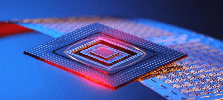
In the morning Qualcomm’s Beth Keser gave us an introduction to fan-out wafer level packaging (FO-WLP). She demonstrated how essential this technology is, offering both low cost and a small form-factor for mobile devices. Beth had prepared more than 200 excellent slides addressing the materials-, thermal-, mechanical- and of course electrical challenges this packaging technology has to meet, at very low cost. “Thin is clearly in” in mobile devices. I was surprised that IC packages as thin as 0.55 mm can be achieved widely today. – FYI: A penny is 1.5 mm thin!
While manufacturers utilize their unique flows to differentiate their wafer-level packaging capabilities, the simplified key steps of processing a wafer right out of the wafer fab are:
- Wafer probe.
- Wafer thinning.
- Wafer dicing.
- Arranging the good dies, face down, on a carrier (in wafer or panel form) with copper pillars or solder joints and interconnects.
- Reflow.
- Backside interconnects and under-ball-metal, if needed.
- Ball attach on the backside.
- Mold-compound to cover dies and gaps between them.
- Package singulation.
- Final test.
Except steps 4 and 10, all other processing steps are performed on a wafer-level for 100s if not 1000s of chips in parallel. This significantly reduces unit cost, compared with die-to-die or die-to-wafer assembly, and makes this technology attractive for high-volume and cost-sensitive applications, like smart phones and other mobile devices.
Beth also explained that FOWLP allows us to combine a few dies in a package; a low cost alternative to an interposer design. As an example, she showed key parameters of TSMC’s InFO package:
- L/S down to 2/2 μm.
- Up to 15×15 mm die size for a single die.
- Up to 8×8 mm for up to 4 dies.
- Down to 0.45 mm thin package.
- PoP is supported.
In addition to highlighting TSMC’s packaging strengths, Beth showed FO-WLP capabilities and design rules from major assembly houses and IDMs, even outlined AT & S’ ability to embed dies into printed circuit boards (PCBs).
In the materials section Beth talked about characteristics and challenges of Epoxy Mold Compounds (EMC), carrier warpage and the impact of manufacturing temperature profiles on different materials. She covered manufacturing equipment for FO-WLP next, showed design rules from different manufacturers and demonstrated her competence in reliability tests.
Last, but not least, Beth showed a number of roadmaps and FO-WLP cost projects. She emphasized again that low cost, the ability to customize and a small formfactor are packages’ key criteria for success in mobile applications.
Tuesday afternoon Luu Nguyen from Texas Instruments showed us, like Beth, his vast packaging experience. He started by taking us on a tour back in history. He showed how rapidly cell phones have driven advances in packaging technology and how the need for integration of heterogeneous functions will continue to drive investments in single- and especially multi-die packaging. While application processors (APUs), modems and graphics chips will benefit from continued shrinking of feature sizes, economics suggest to implement RF, power management (PMIC), MEMS, imagers and analog functions in process technologies with larger feature sizes to reduce development- and unit cost, in addition to saving time to market.
Like Beth, Lou showed us examples of how many companies use packaging technology to gain technical- and cost advantages. He highlighted Tessera/Invensas and Flip Chip International as companies who license their packaging know-how to others and showed how flip chip technology and chip scale packaging have advanced semiconductor capabilities. Lou also commented on the benefits and trade-offs of the many different packaging technologies, talked about material characteristics, assembly- and test equipment, reliability tests and failure analysis.
If anyone still viewed IC packaging as a simple and low-tech domain last Tuesday morning, after attending these two short courses about advanced packaging, they certainly realized that the experts who drive IC packaging innovation deserve a lot of credit and respect.
While ECTC offered on Tuesday a total of 16 professional development courses, on Wednesday, Thursday, and Friday it offered six tracks of packaging related presentations, panels, lunch-time keynotes and opportunities for networking.

The most impressive keynote I was able to attend at ECTC was from Matthew Grob, Qualcomm’s CTO, on Wednesday noon. He started his talk with a very bold statement: “We need 1000 times the communications bandwidth in 10 years” and conveyed that Qualcomm is committed to getting there. Matt outlined how faster and more reliable wireless technology will transform cities, hospitals, manufacturing facilities, homes and many other aspects of our lives. He predicted that by 2018 about 60% of new cars will be smart, connected and much safer than today’s cars. They’ll communicate vehicle to vehicle and recognize pedestrians to avoid accidents. They’ll even communicate with a city’s infrastructure to find parking, avoid traffic jams automatically, park themselves and do a few other things “Knight Rider” episodes showed on TV years ago.
As I mentioned above, my focus at ECTC was the “Advanced Packaging” track, even when I had to stand in the back for an entire presentation or even a complete session. Let me share with you some of my ECTC general impressions:
- Innovative low-cost packaging technology (e.g. FO-WLP) and interposer-based designs find broad market acceptance.
- Vertical die-stacking (3D-ICs) is currently only utilized for combining identical memory dies from the same wafer fab.
- Partitioning logic into multiple, stacked dies appears to have a very slow start at a few large companies, who prefer not to make noise about their ongoing developments. Likewise, examples for stacking DRAMs on top of logic are rare.
This trend reminds of what I learned in my 20+ years in the ASIC business: Customers always want better technology AND lower cost — and, as we all know, customers rule!
I may have to rename my company from “eda 2 asic” to “eda 2 packaging”. While all ASIC and other IC designers can’t live without EDA tools and productive IC design flows today, the relationship between the packaging- and EDA segments of our industry needs to be further improved. It is currently were the relationship between the ASIC and EDA segments was, when in 1996, I changed from VLSI Technology’s ASIC business to Viewlogic’s EDA tools to proliferate Viewlogic’s and later Synopsys’ tools into many companies’ ASIC design flows. Why am I saying this? When I attended Stephen Pan’s excellent presentation about ANSYS’ EDA capabilities to model and simulate the impact of temperature on electro-migration and how to avoid power- and signal integrity problems, the room was less than half full. The only encouraging sign that we are heading in the right direction was the average age of the relatively small audience. Many of them were about half my age and saw that designing of cost-effective ICs, getting to market on time, avoiding re-spins as well as yield loss surprises and reliability problems demands package modeling- and IC design tools.
IC- and package designers need more powerful tools now, and to a much greater extent in future. These IC- and package design tools need to work well together and enable designers to consider during IC planning, design and verification the technical- and business considerations of the package on their silicon design. I am optimistic that EDA- and Packaging experts will work together to address the “eda 2 packaging” co-design challenge in the next 20 years and show similar progress as ASIC design flows did in the last 20 years.
If you want to know more about this co-design challenge and emerging solutions, please come on Monday, June 8, to the Si2 Booth (# 814) at the Design Automation Conference (DAC 2015), as well as the die-package co-design panel (# 1-9-7) I’ll moderate at InterPACK on July 9. My co-design presentation that afternoon will address this critical topic. For the 3D ASIP conference I’ll organize a ½ day session on December 15 to address exactly this and other modeling- and design challenges, with help from my friends in EDA firms and IC packaging companies. All three of these events are in or very near San Francisco and definitely worth attending.
Talking with Exhibitors was another important part of ECTC. In two large tents in the hotel’s parking lot more than 100 exhibitors showed their current capabilities, outlined their plans and captured what potential customers were looking for in future. Several R & D organizations, many material suppliers, manufacturing and metrology equipment vendors, assembly & test houses (OSATs) and a few EDA vendors — CST, eSystem Design, Mentor Graphics and Zuken — demonstrated their IC- and Package design tools.
To report about the many “Advanced Packaging” presentations I attended has to wait for my second part of ECTC reporting in the very near future. I hope to see you at DAC next week to discuss chip-package co-design! ~ Herb


