
 In the Jan/Feb issue of ChipScale Review, there were two interesting articles on fan-out wafer-level packaging (FO-WLP) entitled “Eliminating Warpage for FOWLP during Debonding” by ERS Electronic GmbH and “Overcoming FOPLP Die Placement Error” by Onto Innovation …lets take a closer look.
Eliminating Warpage for FOWLP during Debonding
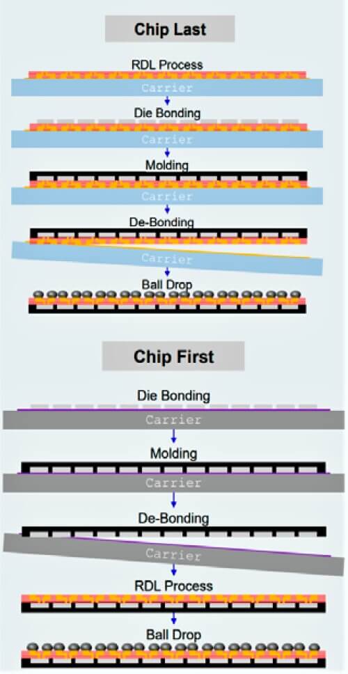
As we all know, FOWLP can be done RDL-first or dies first as shown in Figure 1. In the chips-first approach, the RDL is formed on the reconstituted wafer after release from the carrier, whereas in the RDL-first approach the redistribution layer RDL is formed on a wafer flat surface. Chips first is used commercially by Infineon, ASE and Deca Technologies, and chips-last is used for high-density solutions like TSMC’s integrated fan-out (InFO).
Two critical issues exist for FOWLP: die shift and wafer warpage. Die shift results from displacement of the die with regards to its designed position. Warpage is due to the mismatch of the CTE between silicon and the epoxy molding compound (EMC). The EMC, having a higher CTE value, and being placed on only one side of the silicon, results in an imbalance, which will cause the wafer (or panel) to warp after debonding (separation of the reconstituted wafer from the carrier). This CTE mismatch creates an imbalance in the expansion and contraction during subsequent thermal processes. This affects both issues regarding handling and automation and yield, where it can cause high thickness variation during the coating process, or pattern defects during exposure.
The authors have found that applying a thermal treatment process, can result in a warpage profile <1mm, which allows succeeding processing.
The warpage adjustment concept described in this paper, and developed by ERS Electronic GmbH, is known as “shock and lock.” The wafer is subjected to a temperature equal to or higher than its Tg for a predetermined dwell time, After the wafer is exposed to this heating, it is transported to a cold thermal vacuum chuck, and the profile locked in as the wafer cools.
They examined:
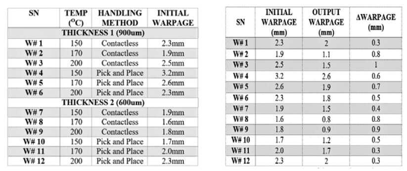
- Warpage adjust temperature (150°C, 170°C and 200°C)
- Wafer thickness
- Wafer handling method
The handling method being the technique used to transport the wafer to the cooling chuck. Contactless transport involves transport without contact such as Bernoulli handling and AirCushion handling.
Warpage improvement was observed in all the samples tested as shown in Table 1. The best results were for the highest reset temperature in combination with contactless handling.
Overcoming FOPLP Die Placement Error
The other critical challenge for FOWLP, especially using panel level processing (PLP), is die placement error, which occurs when the dies are positioned during the reconstitution and molding process. Generating reconstituted panel substrates creates translational and rotational die placement errors. The “pick-and-place” process itself introduces initial errors that are magnified by the instability of the mold compound throughout thermal processing. With RDL features currently achieving dimensions as small as 2μm, tolerances are getting tighter and tighter.

These placement errors are amplified by the larger panel processing format and positional errors of 50μm or more have been reported. In order to guarantee acceptable yield, these errors must be corrected during the lithography process.
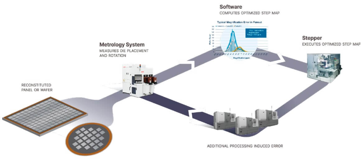
Thus, the position of the die must be measured before each exposure in the lithography system to ensure accurate registration with the underlying layer. Displacement errors can be measured in the lithography tool, but these measurements are slow, typically taking as much time as the exposure itself. Obviously conducting metrology and site-by-site exposures on the lithography system is quite time consuming, reducing throughput and increasing cost enough to make the approach impractical.
The new approach uses an external metrology tool to capture die placement error data from a panel and feeds that information forward. The “feed-forward” solution optimizes the stepper, site-by-site, for X, Y and rotation offsets, during exposure (See Feature Photo above – courtesy of Onto Innovation.)
As long as the measured errors are within the correction capability of the stepper, it is possible to yield 100% by correcting each die, so-called “die-by-die” exposure individually, but this imposes an unacceptable penalty on stepper throughput. Increasing the size of the exposure to cover multiple die will increase throughput, but reduces the ability to correct for individual die placement errors. AOI pre-measurement of panels with product die can be used to determine the optimum field size, throughput and yield prior to coating the RDL processing step.
Onto Innovation’s software algorithm for the panels evaluated, predicted 100% yield with a field size of 3×3. The software algorithm’s yield prediction was compared to actual customer product overlay measurements, confirming the accuracy of the prediction is within 0.2% of final overlay results.
For all the latest in Advanced Packaging stay linked to IFTLE…………………..


