First… the manufacturing process
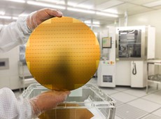
Microelectronic components and semiconductors are manufactured on round thin discs, referred to as wafers. Wafers can be made of various conductive or non-conductive materials such as silicon, sapphire, or glass with a typical diameter of 100, 150, 200, or 300 mm.
The blank wafers are subjected to various etching, grinding, and polishing processes in the manufacturing process. The wafers are given an almost perfectly flat surface by these production processes. The components and structures are produced by a repeated sequence of additional structuring and deposition processes.
From the initial product ingot to high-quality wafers
Manufacturers in the fields of microelectronics, microsystems technology, and photovoltaics have high demands on the production tolerances of the pre-product “wafer”. Even small deviations can have a negative impact on the quality in the downstream, cost-intensive process steps. This results in lower yields and reduced efficiency and reliability of the end products. High-quality, fully automatic multi-sensor measuring technology contributes to the control of process tolerances in wafer manufacturing and helps to maintain the required quality standards of the producers.
Sawing, grinding, and polishing – Tolerances and standards in wafer processing
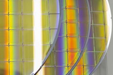
 Wafers are the substrate for the production of integrated circuits, light-emitting diodes, micromechanical (MEMS) components, and solar cells. The particularly fine thin wafers are required primarily for the manufacture of 3D IC components. The micrometer-sized circuit packages are created by stacking and connecting in a vertical direction. Microchips mounted on thin wafers are assembled. This miniaturization allows even more efficient circuits to be realized, for example, for more efficient solid-state disks, more compact CMOS image sensors, and more powerful and energy-efficient logic components. The requirements for the specifications of the output product wafers are immense. Sawing, grinding, and polishing require maximum precision.
Sawing the starting product
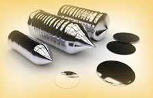
The ingot, a block of semiconductor material (e.g. silicon) or a compound material (e.g. Gallium Arsenide (GaAs)), is the starting material for wafer production. As a rule, the ingot is drawn from the melt, usually using the Czochralski process, and doped during this process.
With a high-precision wafer saw, individual raw wafers are cut from it. This creates grooves whose width and depth must be checked. Optical measuring systems with multi-sensor configurations are ideal for this task. The saw contour cannot only be visualized three-dimensionally but also quantitatively and metrologically characterized – a task in which classical optical microscopes reach their limits. The quantitative measurement allows the sawing process to be better controlled so that the deviations in this process step are significantly lower. In addition, the tool wear of the processing machines can be monitored and the behavior of different materials during the sawing process can be evaluated.
Grinding evenly
 After sawing the wafers are thinned using mechanical processes such as grinding and lapping. During the grinding of a raw wafer or structured wafer, certain quality parameters must be maintained. For raw wafers, for example, the TTV value indicates uniform removal during grinding. The TTV value is a statistical value based on a metrological wafer thickness measurement indicating the absolute thickness variation of the entire wafer. The point here is to determine the maximum difference between the thickest and thinnest point, the so-called Total Thickness Variation (TTV).
Smooth polishing
 In the thin wafer polishing process, a polishing pad applies pressure to make contact with the wafer surface and polishes it. A polishing paste (slurry) containing chemically effective substances and abrasive materials is used. The removal of the wafer surface occurs by friction. In a dry-polish process, the chemical and abrasive material is bound in a pad. In this process, lower contact pressure is sufficient. Optical measuring systems are used for monitoring the polishing process because the determination of the roughness allows conclusions to be made about the surface quality.
It has to be flat: The perfect wafer
The surface finish of the wafer is characterized by its flatness. The flatter the surface, the more perfect the wafer is. Differences in height may lead to contacting problems during subsequent stacking to a 3D IC wafer package.
 In addition, the wafers must be ground to an exact thickness and the doping introduced into the substrate should not be removed too far. The wafer edge can also be checked at random with a 2D profile measurement. From this, the wafer manufacturer can determine the wear of the grinding tools and optimize the process parameters. Waste at the edge of the wafer also plays an important role. The more efficiently this is done, the more microchips can be produced on the wafer later, and the so-called fill factor increases. Processed wafers that are equipped with bump structures or solder balls, for example, can be measured in terms of height, width, and coplanarity.
Special Interest: Advanced microchip packaging
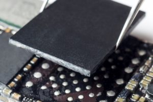 Advanced packaging technologies are rapidly evolving in the semiconductor industry to achieve the functionality, speed, and form factor required for the mobile market.
As wafer-level packaging (WLP) and heterogeneous integration (HI) approaches become more relevant, metrology processes begin to creep into back-end process control, where measurement becomes trickier and more diversified. The dawn of fan-out (FO) processes both at the wafer and panel level has added more diversity to metrology needs. The addition of 2.5D and 3D heterogeneous integration, and now chiplet technologies further expands the diversity of applications.

The fabrication of an integrated circuit (IC) requires a variety of physical and chemical processes performed on a semiconductor (e.g., silicon) substrate. By creating structures of various components, millions of transistors can be built and wired together to form the complex circuitry of a modern microelectronic device.
Three-dimensional integrated circuits (3D IC) and 2.5D IC with Si interposer are regarded as promising candidates to overcome the limitations of Moore’s law because of their advantages of lower power consumption, smaller form factor, higher performance, and higher function density. To achieve 3D and 2.5D IC integrations, several key technologies are required. The cost and complexity of these new packaging technologies require cost-effective inspection and surface metrology solutions across the entire process to ensure product quality and yield.
Meet the measurement requirements
Whether for measurements with several layers, for example with bonded or taped wafers, edge evaluation of the wafers, or the evaluation of the coplanarity of bump structures, with modern optical measuring systems you can easily measure your wafers with high accuracy and keep pace with the increasing demands on accuracy and reproducibility.
(Total Thickness Variation) TTV setup: Option for a two-sided sample inspection
The system can be equipped with an opposed sensor configuration (TTV setup) consisting of two non-contact chromatic white light sensors.
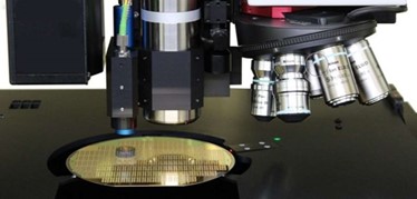
It is possible to measure both the roughness and the TTV with very high resolution using the FRT MicroProf® surface metrology tool.
This multi-sensor surface metrology tool measures the complete wafer surface and determines thickness, TTV, bow, warp and flatness as well as high-resolution 3D topography, 2D profile, and roughness measurements. The optical sensors are fast and very accurate. Furthermore, the system can be equipped with Atomic Force Microscope (AFM).
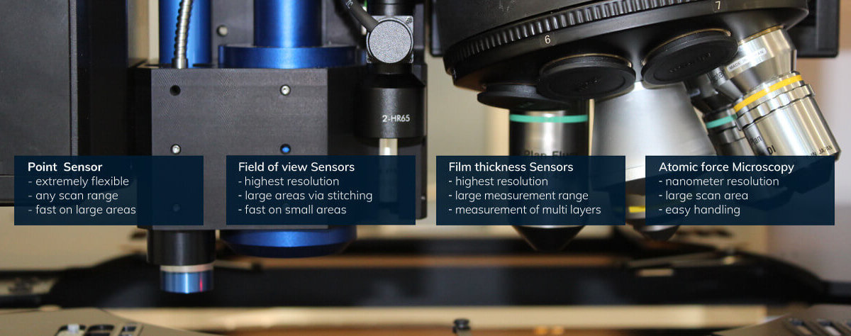
SurfaceSens surface metrology concept
 Based on our SurfaceSens concept, the 3D surface metrology measuring devices can be equipped with point, line, and field of view sensors for topography analysis as well as with film thickness sensors. In addition, atomic force microscopy can also be applied. As a result, complex measurement tasks can be solved with the use of different sensors by collecting the data from each sensor and subsequently combining the different results.
The decisive step is now that the instrument, respectively the recipe used, knows the complete measuring task and fully implements it. This means not only the data collection with all necessary sensors is automated, but the software also records the different results and calculates the desired parameters.
Hybrid metrology: Determine parameters that cannot be measured directly!
A hybrid measuring concept increases the precision of measurements on samples for which a single sensor or a single measuring principle is simply not enough. Depending on the application, it can include measurements with different topography and (layer) thickness sensors, which are fully automated by a single recipe. Controlled by FRT software, these sensors automatically acquire different data sets to create new information by combining data that is not directly accessible with a single sensor.
The MicroProf® series: standard and special solutions to improve your production efficiency
Whether you need a standalone, non-contact wafer measuring tool for your lab or a fully automated, integrated tool in your front-end or back-end areas, FRT offers the appropriate standard and special solutions to improve your production efficiency. The degree of automation extends from manually operated or semi-automated tools such as the MicroProf® 300, to fully automated tools with wafer handling. It includes automatic pre- and fine alignment in the MicroProf® MHU for very high-volume processing of microelectronics and wafers. Further options are the handling of thin wafers and an ionizer bar.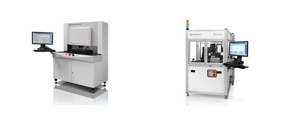 In addition, tools can be equipped with powerful image acquisition hardware for intelligent pattern recognition. FRT surface metrology systems can be configured to handle SEMI-compliant and non-standard wafers often used in the MEMS industry. We also offer a variety of solutions for the growing market segment of 3D IC manufacturing from thin-film measurement to trench measurement to inspection of critical dimensions in the whole manufacturing process.
For semiconductor applications, FRT offers tools for cleanroom manufacturing: the MicroProf® FE, MicroProf® FS, and MicroProf® AP. As a standard, the MicroProf® tools are equipped with filter fan units (FFU) that ensure ISO Class 3 cleanroom conditions within the unit.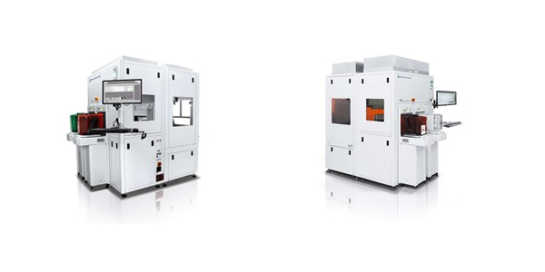 The MicroProf® can process 150/200 mm and 200/300 mm wafers in one system (FOUP, SMIF and open wafer cassettes possible). The SEMI-compliant software GUI enables interactive or automated use, easy creation of measurement and evaluation recipes, and integration into existing production control systems via the SEMI-compliant SECS/GEM interface. This interface transfers measurement information to the next step in the production line.
For more information, please visit the Metrology section of our website.