

Fan-out wafer level packaging’s star is clearly on the rise as a low-cost solution for consumer mobile products, and the semiconductor industry trade news has been buzzing with unsubstantiated claims that Qualcomm is ditching through silicon vias (TSVs) for monolithic 3D ICs (M3D) in its next generation of cell phones. Meanwhile, it seems 3D TSV technologies have been moved to the back burner until the cost comes down sufficiently for high volume implementation. In fact, by the looks of things, one might surmise that combined, FOWLP and M3D could put 3D TSVs of the running for consumer applications altogether. But is that really the case? I decided it was time tap into our experts on the 3D InCites Technical Advisory Board to gain some perspective.
FOWLP vs. 3D TSV
According to the 2015 Yole Développement report on FOWLP and embedded die, “the market is worth almost $200M and we anticipate 30% CAGR is in coming years”. In a recent i-Micronews interview on the topic, David Butler, SPTS, broke down the market in three segments (allowing for some overlap): 3DIC (3D TSVs) for high performance, where cost considerations are secondary; FOWLP for high density applications, where cost matters; and finally wire bonding, which is not going to disappear. There will be areas of overlap of course. “The relative success of 3D IC vs FOWLP will partly depend on who gets into high volume first,” Butler says.
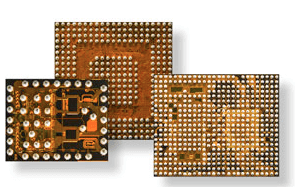
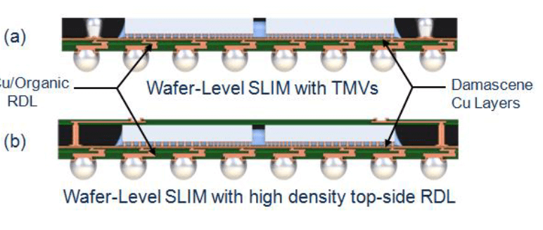
We know that FOWLP technology development continues to evolve in an effort to achieve tighter lines and spaces. In fact, in the years since Infineon, ST Microelectronics, STATS ChipPAC and Nanium launched (and licensed) eWLB, other companies have jumped in mix with their versions of FOWLP including Deca Technologies with its M-Series CSP, Intel with its embedded multi-die interconnect bridge (“EMIB”) packaging technology, SPIL/Xilinx with its silicon-less interconnect technology (SLIT), TSMC with its integrated fan-out wafer level package (InFO-WLP) and, most recently, Amkor’s silicon-less integrated module (SLIM), which the company introduced in March at IMAPS DPC, with claims that it achieves .5µm line/space (Figure 2).
While FOWLP is clearly giving 3D TSV technology a run for the money, will it ever reach the densities that can be achieved by 3D IC with TSVs?
The simple answer was a resounding “no” across the 3D InCites technical advisory board. But there’s actually a lot more to it than a simple yes or no answer.
“FOWLP will never reach TSV densities unless people spend more money on more advanced FOWLP tools – which kind of defeats the purpose,” noted Paul Werbaneth, 3D+.
Jan Vardaman, Techsearch International, Inc. says that the current density limit of FOWLP in production is around 10µm line and space, and maybe a little less. The features sizes for 3D IC or 2.5D silicon interposer and even some of the alternatives are 2µm or less. “The main question for consumer options today is what density is required and which technology can provide that density for the lowest cost,” she said.
Additionally, Larry Smith, independent consultant, 3D TSV technologies, pointed out that we are comparing a perimeter interconnect (FOWLP) with an area array interconnect (TSV). “The relative number of connections depends on the die size. Additionally, TSVs allow very short, direct connections from the interior of one die to another die or to an interposer, which can be very important for power distribution, power consumption, and/or signal integrity,” he explained. “This (comparing FOWLP with 3D TSVs) is analogous to comparing fine pitch wire bonding with flip chip.”
Regardless of the wiring densities, different applications need different numbers of transistors packed into one IC package, noted Herb Reiter, eda2asic. “FOWLP is a low-cost technology with limited flexibility. There are limits on the numbers of die, package pins, and interconnects between dies. Also, the maximum max power dissipation is currently only 1 to 2 Watts,” he explained. “Alternatively, 3D ICs can integrated many more die, limited only by the ability of the package to get the heat out. It allows many more interconnects between dies (I have heard of a 3 D stack with 10,000 interconnects), can integrate much more functionality and have many more inputs and outputs – as the package allows. However, complex 3DICs can get MUCH MORE expensive that FOWLP.”
“Both integration techniques address different product categories,” said Jürgen Wolf, Fraunhofer IZM-ASSID, “There is definitely a trend for multiple die integration using FOWLP, but these generally involve standard available ICs or passives. There also seems to be a trend to merge 3D IC and FOWLP for some SiP applications.”
Will consumer products ever reach the point where even FOWLP isn’t enough to meet performance and power requirements? Rozalia Beica, Yole Développement says it’s still too soon to tell, and that it will depend on the particular product. For example, she said Yole just had some teardowns done on top smartphones and still didn’t find a single FOWLP inside.
M3D vs. 3D TSV
We’ve also heard a lot about M3D, and how Qualcomm is supporting research at CEA-Leti, and that CEA-Leti has made progress with CoolCube. According to a recent presentation by Karim Arabi, vice president of engineering at Qualcomm speaking at the International Symposium on Physical Design, the company is hoping to tape out a 3D SOC test chip manufactured using M3D as soon as 2016, however real products will take longer. (This was a correction made at the end of this EETimes post by R. Colin Johnson). Some have interpreted this comment to mean that Qualcomm would be implementing M3D as soon as 2016 for its smart phones. However, this is has not been officially announced by the company. That’s not to say M3D isn’t an important advancement, it’s just not ready for prime time.
My question to the advisiory board: Will M3D be ready for commercialization before the cost of 3D IC using 3D TSVs come down?
Again, the simple answer was “no”, but there was more to it than that.
“Keep in mind that this comparison only makes sense when comparing monolithic to wafer-to-wafer 3D, which restricts us to applications where one company makes all the wafers in the stack, the die sizes match, and the wafer yields are very high,” said Smith.

“I see more complexity in M3D than 3D IC with TSVs, which already is well known and the industry has worked on it and optimized for so many years,” said Beica,
Wolf concurred, adding that major activities in TSV integration are currently driven by Cu-TSV. This includes heterogeneous 3D integration. “All major foundries including Samsung, and GlobalFoundries are ready for product integration (of 3D IC with TSVs). Monolithic 3D IC integration will be only driven by performance applications. Because of the much higher cost I do not see this in HVM yet,” he said.
However, Reiter reminded me that cost is not the only differentiator here. “Monolithic will allow MUCH faster and MUCH lower power dissipation vs 3D ICs and because of these benefits will win in high speed applications, even if they are more costly,” he said, adding that Tezzaron’s 1µm tungsten TSVs are another attractive alternative in between 3DIC and M3D.
Peter Ramm, Fraunhofer EMFT agreed with Reiter on the topic of tungsten-filled TSVs: “3DIC with CVD TSV explicitly using tungsten is unbeatable for performance and density,” he noted. “In some applications when only medium integration density needed, the lateral dimensions of the TSV must be in the sub-um region – especially for heterogeneous integration.” To illustrate his point, he noted Fraunhofer EMFTs 3D TSV process development for IoT applications. Both Reiter and Ramm noted that currently, the only 3DIC processes in real production use W TSV: Tezzaron and IBM.
Everyone agreed that M3D will not be a lower cost solution than 3D TSVs, at least not in the beginning. “Monolithic IC integration is the most expensive one and will stay it in the near future as well,” said Wolf. We all know that Qualcomm is so cost-sensitive, its still using package in package (PoP) in its handsets because the cost/performance ratio is still sufficient. Why would they move to a solution that’s even more costly than 3D TSV stacks?
So to my original point of this article, is it likely that FOWLP and M3D will squeeze 3D TSVs out of the running for consumer applications? While most agreed that FOWLP may keep 3D TSV out of cost-sensitive applications, it’s really too soon to even talk about it with M3D.
“They all have very different technical capabilities, need different EDA design tools, different NRE cost, different development times, more or less ability to re-use existing IP (on the bare die level). The chances to guess right what will win when for which applications are VERY slim.” said Reiter. “There are too many moving variables to predict an outcome.”
“I also see a current trend in a combination of 3D IC and FOWLP,” said Wolf. “The issue for 3D IC currently is the cost of TSV integration, which has to come down and which is mostly related to TSV dimensions, handling, and assembly processes.”
Werbaneth noted that true 3D IC is already in the iPhone camera modules. “If it cost too much it wouldn’t be there,” he said.” It’s also in Avago FBAR filters in handsets at well below $1 per unit. Show me where monolithic or FOWLP is … can’t seem to find it.”
With regard to M3D, technology readiness is not predictable today, said Ramm. Beica added that while M3D has been in the news for some time, adoption is really lacking so there must be a reason for it. “It is not a proven technology yet. We will still watch it and monitor the progress it makes over the next few years.” She said. “Just compare the companies trying monolithic vs. 3DIC and I think you get the answer.”
So there’s your reality check, straight from the experts. FOWLP is definitely the current front-runner for consumer applications. If and when the cost comes down, 3D TSVs are still the next in line and will exceed FOWLP performance and power. And I wouldn’t put money on M3D being in the next-generation Qualcomm smartphone. It’s still the new kid on the block and has a lot of growing up to do. ~ F.v.T.


Read the article and couldn’t figure out why M3D is assumed to be very costly. Newly developed M3D concept will have total cost of ownership comparable to 2D ICs. stay tuned 😉