
The IMAPS International Symposium took place this year in Boston. Let’s take a look at a few of the more interesting presentations that were given there.
Ferric and TSMCs Partner on Voltage Regulators
In their paper “Package Voltage Regulators: An Answer for Power Management Challenges” Ferric describes their package voltage regulators (PVRs) that reportedly are the industry’s first single-chip power converters with on-chip thin-film magnetic power inductors, which eliminate the need for bulky external components.
A full library of inductor designs spanning a broad range of current, voltage and density requirements is available through Ferric’s foundry partner, TSMC. Ferric’s patented thin-film magnetic core inductors are integrated on top of the chip or interposer as shown in Figure 1.
Ferric’s Integrated Voltage Regulator system designs are available for monolithic integrated voltage regulator (MVR) implementations in TSMC N28 and N7 (in development).
The conduction of power to a high-performance IC typically requires nearly 50% of package and IC I/O and is increasing with lower supply voltages and higher power density in more advanced CMOS nodes. By performing power conversion and voltage regulation in a package, the limitation can be mitigated. Ferrics integration of thin-film ferromagnetic inductors with CMOS technology enables power converters to be packaged with processors, HBM memory and other functions.
PVR Advantages
Since the integrated inductors in the PVRs are fabricated using CMOS BEOL layers, the power MOSFETS and control circuits of the power converter can be located directly below the inductors, leading to dense solutions, i.e as thin as 0.2mm. By decreasing the amount of current that must be delivered to a SoC package, PVRs can significantly reduce the number of package I/Os required for power and ground. Additionally, resistive losses in power distribution networks can be mitigated by the inclusion of PVRs.
In July 2018 Ferric was awarded $3.1M award as part of DARPA’s Electronics Resurgence Initiative (ERI) to develop products in the area of integrated power management for novel compute, with focus on:
- New materials and component technologies that enable novel compute topologies
- Circuits prototypes and architectures that leverage unique components and functions
Namics
High-power semiconductor applications require a thermal interface die attach material with high thermal conductivity (TC) to efficiently transfer the heat generated by these devices. Current thermal interface materials (TIMs) such as thermal greases, thermal pads and silicones reportedly do not deliver high enough TC for today’s power devices. At the recent IMAPS meeting in Boston, Namics, well known for its underfills, discussed the potential of using low modulus sintered silver die-attach and Ag/epoxy thermal interface materials for high power semiconductors.

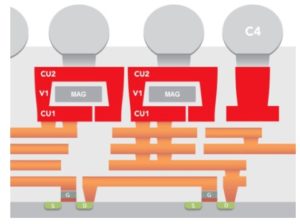
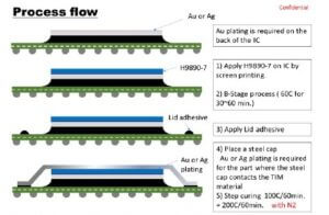
Normally sintering-type silver pastes show excellent thermal and electrical performance due to their dense silver structure but cure temps of > 400°C are required for the sintering. Low temp cure type silver pastes show less stress development and heat damage but have limited TC due to poor continuity of the silver in the paste. Using nanosilver particles generated by decomposition of organo-silver compounds, Namics was able to develop a 90 min cure at 175°C material (H9890-7) with a viscosity of 60 Pa sec and 83% silver. This results in a TIM with 70 W/mK TC. The porous sintered structure of the fused nanosilver was reinforced by a resin system without degrading the high TC (Figure 2).
AIST
The Advanced Industrial Science and Technology group (AIST) at Tsukuba Japan discussed their development of a “Backside Buried Metal” (BBM) layer for global power routing in 3DICs which improves power integrity and overall 3D-IC performance.
The 10um BBM layer for global routing is introduced in the large vacant area on the backside of the die after backside thinning and is connected to the front side through the normal backside via last (9um TSV) technology developed many years ago. The resistance of the power supply and ground lines are shown to decrease. In addition, the BBM acts like a decoupling cap because it is buried in the silicon and has a metal-insulator- silicon structure. The BBM layer is fabricated simultaneously with the signal TSVs.
For all the latest in Advanced Packaging stay linked to IFTLE……………………..


