
As predicted, 2020 will go down as the year 5G hit the big time. But it got off to a rocky start. Back in January, the semiconductor industry—and the world as a whole—had high hopes for the 5G rollout. Then COVID-19 hit, and two things happened.
First, progress on the 5G rollout stalled as standards work was suspended, which was expected to delay device development. But then, data storage and transmission needs increased exponentially as the world settled into a work-from-home and shelter-in-place culture. Additionally, the race to the 5G rollout became a geopolitical issue.
As a result, technology development is going full steam, and we find the industry in transition to catch up to the growing demand for components and subsystems.
The Need for 5G Connectivity
As consumers stream more videos, shop online, videoconference, and get used to telemedicine visits with the doctor, our dependence on connectivity is exploding, and 4G/LTE networks can’t keep up. Moreover, the race is on to implement artificial intelligence across a plethora of devices that need 5G connectivity. This is driving the industry to revolutionize broadband services and empower connectivity across end-user verticals.
The Race to the 5G Rollout
On the geopolitical front, the 5G rollout was delayed in Europe and the U.S. However, Korea, China, India, and other Asian nations have made significant capital investments in the 5G infrastructure and are actively rolling it out. Saudi Arabia reportedly boasts the fastest download speeds, and South Korea has the highest rate of adoption.
In late summer, to help speed the U.S. rollout of 5G, the White House and the Department of Defense announced a plan to share a portion of their mid-band spectrum with the wireless industry, all though it’s not expected to go into effect until late 2021.
On the handset side, now that the infrastructures have expanded, Apple finally introduced its 5G iPhone. Across the board, the volumes of 5G handsets sold are increasing.
Technology Trends for 5G Components and Subsystems
Providing end-to-end 5G connectivity requires a network designed to use all spectrums and bands. As a result, we’re seeing a shift to incorporating higher frequency bands while still accommodating other bands (3G, 4G, LTE, etc.) into components and subsystems. This is because mmWave technology, considered to be true 5G, can only travel a short distance. Therefore, its use will be limited to urban areas where femtocells can be placed in close proximity.
Not only are the increased handset volumes impacting the component and subsystem makers, but the increased amount of content is too. Handset manufacturers are calling for fully integrated subsystems featuring low power consumption to accommodate the need for size reduction, all at a competitive cost.
RF Filters and Power Amplifiers
Two key devices used in both networking infrastructure and handsets are RF filters and power amplifiers. 5G has different requirements for these components than those used in previous generations of wireless technology.
For example, RF filters must have improved filtering performance through lower losses and steeper frequency cut-offs. In addition, filters must be designed for higher frequencies associated with 5G, and exhibit performance stability under a wide range of temperatures and environmental conditions. This ensures that the guard bands between useable frequencies, as well as the duplexer gap (the transition space between transmitted and received frequencies) can be minimized.
Power amplifiers in handsets will continue to use gallium arsenide (GaAs) technology. Gallium nitride (GaN) power amplifiers are the best choice for base stations as they enable high power density in a small form factor. We’re also seeing a higher level of antenna-in-package (AiP) power amplifier integration.
Changing the Processes
These technology macro trends are impacting the device manufacturing process in several ways. Overall, manufacturers need to accommodate GaAs and GaN substrate materials. Doping the materials is needed to prevent insertion loss. Manufacturers also need to adjust processes to accommodate a reduction in material resistance. Lastly, thinner layer deposition is needed to enable higher frequencies.

Process Tool Adjustments
Accommodating the process changes for manufacturing RF devices and power amplifiers for 5G applications call for tools that are up to the challenge. They must handle multiple wafer sizes, from 6 to 8 inches. Achieving steep cutoffs in RF filters means improved etch-quality profile and uniformity. Thinner layers call for improved deposition, as well as pinhole-free, ultra-thin passivation layers. Additionally, run-to-run repeatability is essential to meet high productivity at a low cost of ownership, as well as to meet volume requirements.
Up to the Challenge
Veeco offers a breadth of process technologies to support the full spectrum of device manufacturing needs, including wet processes, lithography, ion beam etch (IBE), atomic layer deposition (ALD), and metalorganic chemical vapor deposition (MOCVD). This suite of process tool solutions provides high performance at a low cost of ownership to build devices that go into consumer products. All systems support flexible wafer size systems and achieve uniform thickness with precision.
Wet Processing
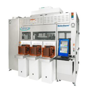
Of all the tools in Veeco’s lineup, Veeco’s WaferStorm® is the workhorse for wet processing applications for RF device processes including metal liftoff (MLO) and photo-resist (PR) strip applications. MLO is critical for RF filter manufacturing as a cost-effective alternative to etch processes that can damage underlying substrates.
WaferStorm’s proprietary two-step process incorporates an immersion step followed by a high-pressure spray that is especially effective on PR that is thick and difficult to remove. Additionally, it uses five times less chemistry than conventional batch processes while doubling throughput versus traditional single wafer approaches. Chambers are stackable to accommodate a compact footprint while still supporting high volume needs.
Ion Beam Etch
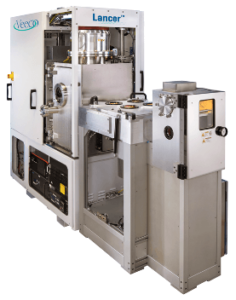
Veeco’s Lancer® platform applies Veeco’s core ion beam etch source technology to RF devices.
With 5G, the doping of piezoelectric material and more complex electrode designs are required in order to improve filter performance. This trend is driving etch challenges related to uniformity, etch profile control, and substrate damage. The Lancer can address these concerns in a production HVM system.
Atomic Layer Deposition
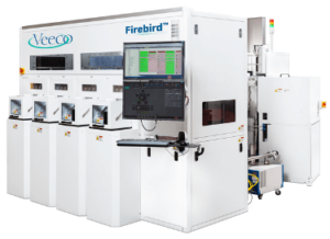
As the material sets for RF devices entail the use of complex piezoelectric materials such as LNO and LTO, atomic layer deposition (ALD) provides a means of obtaining high-stability filter performance through its application as an encapsulation and barrier film. The conformal and dense nature of the ALD films provides excellent protection against environmental degradation thereby ensuring stable operation of the devices. Veeco’s Firebird™ system utilizes a unique handling architecture in combination with controlled environment load locks to realize breakage-free movement of wafers within the system. Additionally, multi-batch operation employing Firebird’s intelligent scheduler enables superior throughput and process consistency, resulting in high-performance RF devices.
Metal-Organic Chemical Vapor Deposition
Power amplifiers (PA) for 5G handsets require high linearity, high efficiency, and high reliability. A key enabler of such devices starts with epitaxial layers consisting of sharp interfaces with uniform doping and composition. MOCVD is the deposition technique of choice for high-volume manufacturing of GaAs-based transistors for handset PAs, due to its ability to grow materials with high uniformity at mass production throughput to give the lowest cost of ownership. Veeco’s Lumina is specifically designed to meet the industry’s latest epitaxial growth requirements and has been proven to provide extremely sharp interfaces with no memory effect, and uniform film layers (within-wafer, wafer-to-wafer, and run-to-run). Coupled with a fast wafer transfer system, high growth rates, fast temperature ramping, and high uptime, Lumina provides the industry’s highest throughput for wafer sizes from two to eight inches.
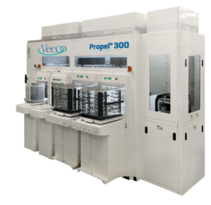
Power amplifiers for base stations require high power and high-frequency performance to allow fast data transmission needed for the 5G network. Current technology for sub 6Hz base stations utilize GaN HEMT on SiC to meet this requirement. However, as 5G progresses to mmWave base stations, high-power microcells with multiple distributed antennas and small cells system will be needed to enable fast data rate transmission. The high volume requirements mean growth on larger wafers size such as 8” and 12” silicon wafers to lower the cost of devices for large scale adoption. Veeco’s Propel™ HVM systems with single wafer TurboDisc® technology and cassette to cassette automation has demonstrated high performance in uniformity and repeatability with the lowest cost of ownership. The cluster system design provides flexibility and productivity and it is the only GaN MOCVD platform currently in the industry that is proven successful to scale to 12” silicon substrate and ready for high volume manufacturing.
Conclusion
The global demand for faster data rates and improved connectivity is expected to increase considerably in the coming years. As the 5G rollout continues across the world, the need for 5G components and subsystems will continue to expand. Manufacturers looking to expand capacity to support this growth must collaborate with their suppliers and share knowledge to develop cost-effective, high volume processes. These companies need to look no further than Veeco to support their 5G process tool needs.