Moving from 2D scaling to heterogeneous integration and 3D packaging is ever-more critical to improving semiconductor device performance. In recent years, advanced packaging technologies have increased in complexity as well as in variability to support a wider range of devices and applications. In this article, we investigate the limitations of traditional lithography methods for advanced packaging and evaluate a new maskless exposure for back-end lithography.
New Challenges for Back-end Lithography
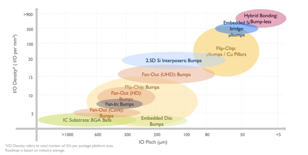
As heterogeneous integration is increasingly adopted for semiconductor development and innovation, back-end lithography requirements are growing, as shown in Figure 1. More redistribution layers (RDLs) within the package are driving the need for finer RDL line/spacing (L/S) as well as smaller critical dimensions for micro-bumps and micro-pillars. This is causing tighter integration design rules at the package and substrate level, which increases the risk of overlay and die shifts that can lead to parasitic effects and yield loss.
At the same time, the number of I/Os is growing to improve package performance, which leads to a larger silicon footprint and reticle stitching. This drives the need for aggressive pitch reductions for I/O bumps and interconnects. Improved overlay accuracy and high depth of focus (DoF) in vertical sidewall patterning are also needed in back-end lithography. New requirements must also be addressed, including minimizing pattern distortion and die shift due to wafer distortion in fan-out wafer-level packaging (FoWLP), as well as patterning on both thick and thin resists while maintaining high DoF and high resolution.
Although the re-integration of larger dies from smaller chiplets has shown numerous advantages over monolithic SoC technologies, including greater freedom of design, this approach shifts the complexity into the integration and with it into the lithography process. Continuous innovation of chiplet design and the variety of integration schemes (on silicon, embedded, or in package) can include several patterning levels, which adds to integration complexity. The increased importance of design flexibility and the ability to simultaneously adopt both die- and wafer-level designs in back-end lithography must also be addressed to shorten development cycles and support the wide variety of advanced packaging platforms.
A Review of Conventional Patterning Approaches
Several exposure methods are available for advanced packaging applications (Figure 2). Among these are mask aligners, which directly expose the pattern onto a substrate through a mask, which is in close proximity to the photo-sensitive, resist-coated wafer. The minimum pattern size is defined by the exposure gap between the mask and wafer. Close proximity of the mask and resist surface will enable smaller patterns; however, too close a gap will cause mask contamination and lead to yield issues.
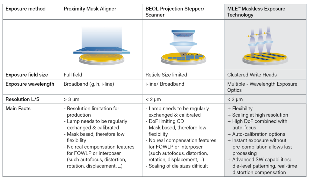
Another exposure method is the back-end-of-line (BEOL) stepper, which uses projection optics between a mask/reticle and wafer to pattern feature sizes smaller than can be accomplished with mask aligners. However, since it is a mask-based exposure method, the stepper must deal with inaccuracies from die placement and die shift variations caused by molding and other factors. In addition, the given reticle size and optics dimensions of static exposure systems limit the exposure area. This can become particularly challenging for larger die interposer fabrication, where stitch lines or mismatched overlap regions of reticle exposure fields can affect electrical properties within the RDL. The ability to generate a stitch-less pattern for interposers exceeding current reticles size is increasingly important for advanced devices that involve complex layouts, such as in advanced graphics processing, artificial intelligence (AI), and high-performance computing (HPC).
In addition, mask-related costs represent a significant additional cost factor to the overall patterning process. Any advanced product design mix, such as those in heterogeneous integration applications, adds to multiple masking levels. As a result, masks and mask inventory/cleanroom storage represent a high portion of overall production costs. Replacement costs for mercury lamps can add up to significant levels. The wait time for new physical mask sets, as well as overall proof of new design concepts for high product-mix designs, intrinsically leads to prolonged development cycles for conventional mask-based production environments.
To address the lithography needs for heterogeneous integration, a new maskless exposure system has been developed, called LITHOSCALE, which features Maskless Exposure (MLE) technology. LITHOSCALE combines high resolution (<2μm L/S) with no exposure field limitations, powerful digital processing that enables real-time data transfer and immediate exposure, and a highly scalable design that supports high-volume manufacturing. The system’s high precision is matched by distortion-free high-intensity optics and sub-nanometer-range stage motion accuracy, which ensures seamless projection across the entire substrate. LITHOSCALE also employs dynamic alignment modes and die-level compensation with an automatic focus in order to adapt to the substrate material and surface variations.
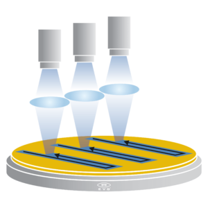
This maskless exposure technology exposes one or multiple wide strips in a parallel scanning fashion and accommodates any wafer size up to panels through a tightly integrated clustered write-head configuration, as shown in Figure 3. A multi-wavelength high-power UV source enables support for all commercially available resists. Throughput is independent of layout complexity and resolution, and the same patterning performance is achieved regardless of photoresist polarity. Finally, the digital mask pattern is projected with sub-micro-second timing accuracy onto the substrate surface. Like most modern lenses, LITHOSCALE imagining system is diffraction-limited, and it supports a depth of field (DoF) of +/- 12μm.
In addition to the wide DoF, the sub-micron precise autofocus extends the usable dynamic focused range to more than 100μm. The ability to control the focus position on a larger scale of the wafer position via chuck positioning and wafer clamping enables compensation for bowed and warped substrates.
Dynamic Exposure Methods and Active Die-level Compensation
Since mask-based lithography methods have no control over distortions smaller than the exposure field, they face difficulties with non-linear, high-order substrate distortions and die-shift-related issues, especially after die reconstitution on the wafer, as is typical for fan-out wafer-level packaging (FOWLP). Lithography experiments were performed employing the dynamic alignment modes on LITHOSCALE in order to evaluate the performance of wafer-level distortion compensation as well as active die patterning on the maskless exposure system.
![[err-ad-fallback-title]](http://www.3dincites.com/wp-content/plugins/a3-lazy-load/assets/images/lazy_placeholder.gif)
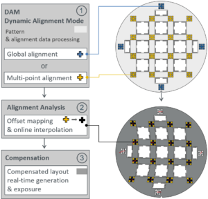
The process flow of the advanced distortion correction function and dynamic alignment modes are visualized in Figure 4. Dynamic alignment includes both global and multi-point wafer alignment options, where typically up to 16 alignment marks (marked with blue and yellow) can be placed randomly in the layout in order to cover the most critical areas on the substrate and compensate for global distortions. After misalignment measurement, displacement vectors are further compiled in parallel before the design is interpolated and rendered in real-time.
The exposed patterns are therefore fully error-compensated without inducing overlapping or noncovered regions – delivering minimum misalignment with no impact on the throughput of the patterning process. A visualization of a compensated layout (dark grey) after an extreme atypical misalignment (indicated with red arrows) example is shown as a result after compensating the actual position of 16 marks (yellow) of multi-point alignment through the dynamic alignment mode.
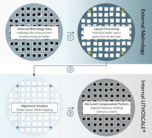
When considering the die distortion errors induced after reconstitution on the wafer, the advanced distortion functionality should also be applied at the die level, where active compensation and re-routing results strictly rely on external metrology data. Distortion compensation algorithms include mathematical correction of rotation, scale, shear, and translation (shift). For die placement error compensation, the model limits distortions within the dies to the rigid body of the die, which typically is represented by two (external) alignment points per die. Due to the immediacy of the conversion process, the dynamic binary pattern generation complements externally acquired metrology data of each die individually per substrate just before the exposure in order to compensate for overlay/positioning errors caused by handling or preprocessing excluding potential thermal influences. A simplified data integrity flow of die-level compensation is visualized in Figure 5.
In parallel, LITHOSCALE enables real-time individualized wafer-level-layout as well as simultaneous structuring of individual die-layouts; in particular, ad hoc die annotations, functional and directly readable encryption codes or active patterning of fuse maps to optimize device binning for process or device tracking and documentation, leading to improved overall yield.
Patterning modularity and vital positioning in sub-grid
The resolution of LITHOSCALE is aimed at typical back-end-of-line resolutions with fine control of the irradiated lines, as well as their gaps (L/S <2μm), while maintaining CD uniformity (CDU <10% CD) and positional accuracy of any arbitrary structures. This precision is matched by the system’s distortion-free optics and stage placement accuracy, which ensures seamless projection across the entire substrate. The exposure can be performed with a very high degree of freedom in intensity control as well as precise light-source-spectrum tuning to achieve optimal absorption and reliable processing for a wide range of commercially established as well as novel photoresists.
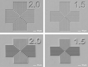
The exposure light source operates at a wavelength spectrum of 375nm and 405nm, allowing for a mix and match of wavelengths to mimic known-good-process recipes or to tailor the exposure to specific customer demands. Both wavelengths can be simultaneously applied in any arbitrary mixture and thus enable thin resist patterning (including positive, negative, polyimide, patternable dielectrics, dry film, or even PCB materials) and also support thick resist exposures at high aspect ratios typically encountered in wafer-level packaging, 3D MEMS patterning, microfluidics, and integrated photonics applications. Figure 6 displays a series of SEM images of standard line-space resolution targets on 1μm thick positive AZ MIR 701 resist on top, while results on the bottom show line-space resolution tests on 2μm thick negative tone resist AZ nLOF. In both cases, a 1.5μm L/S result was achieved through further process optimization involving the reduction of surface reflection effects, which can be achieved by applying anti-reflective coatings or modifying substrate material properties.
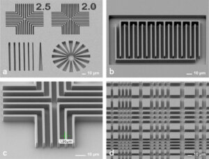
DoF can also be finely controlled to achieve steep sidewalls, and thus keep the desired 3D contour of the resist, or prevent edge topping and footing. A large working distance and automatic adaptive focus ensure patterning uniformity across the exposure surface. Commonly used TOK P-W1000T resist for fine-line and core-line RDL creation was chosen to demonstrate various lines and spacing patterning performance as well as sidewall patterning quality. Figure 7 shows examples of SEM images of baseline evaluation, demonstrating: (A) 2μm L/S resolution targeted on 8μm film thickness, (B) 5μm L/S resolution with meander pattern, (C) spacing variation of 1:2 ratio, and (D) L/S variation in both horizontal and vertical directions with ratios of 1:1, 1:2, 1:3, 1:4.
Summary
The adoption of 3D and heterogeneous integration has led to an increase in package complexity and the number of package options available. Mask-based lithography solutions are no longer practical for many advanced packaging applications as they are unable to make the necessary tradeoffs between resolution and cost, are limited by exposure field sizes, and/or face difficulties with substrate distortions and die-shift-related issues. LITHOSCALE with MLE technology addresses the lithography needs for advanced packaging by combining high resolution with no exposure field limitations, powerful digital processing that enables real-time data transfer and immediate exposure, and a highly scalable design, without the high costs associated with mask-based exposure methods.