Economics are forcing semiconductor manufacturers away from traditional 3D through silicon via (TSV) packaging integration. The future of advanced packaging continues to evolve towards chiplets and innovative new ways to combine specialized microelectronics components. This allows manufacturers to streamline the production for individual “subassemblies” that can then be configured later into functional products.
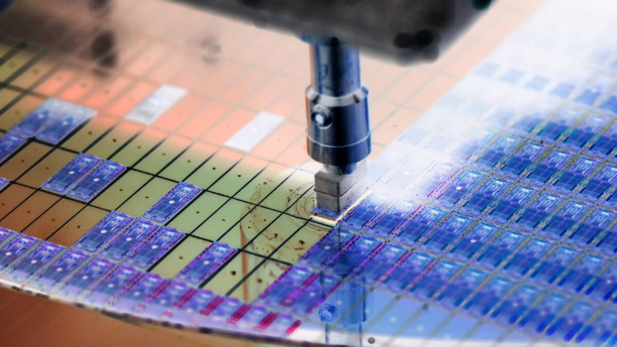
Emerging system-in-package (SiP) designs include not only memory and logic modules, but also MEMS sensors, radio frequency (RF) transceivers, and optoelectronic components. The race to improve chip density is pushing the envelope of flip-chip packaging, requiring double-side processing of the device assembly. Individual chips might come from 300 mm silicon wafers, 100 mm gallium arsenide (GaAs) slices or anything in between.
Due to the varying sizes and interface diversity of the substrates, device wafer handling becomes an issue. Assembling such disparate elements into a single package typically requires temporarily bonding devices to a carrier wafer and performing a number of bonding and debonding steps to process them further down the production line. An intact wafer might be attached to a carrier for backside processing, or for bonding face-to-face with another wafer. Singulated dice might use a temporary carrier for gang-bonding to an interposer.
Wafer Handling Today: Temporary Bonding With Adhesives
Typical bonding approaches for wafer handling include adhesives, waxes, and tapes. Regardless of the application, though, each temporary bond generally requires at least five processing steps:
- Clean the wafer surface
- Coat the wafer, the carrier, or both with an appropriate adhesive
- Align the wafer to the carrier, form the bond, and cure the adhesive
Then, once the temporary bond has served its purpose:
- Use heat, a laser, or mechanical force to separate the two surfaces
- Clean the wafer surface to remove any adhesive residue
Each step poses a damage risk. In all cases, residue and contaminants must be cleaned off of the packaged parts, risking yield loss. Thinned dice and GaAs wafers, in particular, are quite difficult to handle. Bonding and debonding require specialized equipment and unique process chemistries. Also, a mismatch in the coefficient of thermal expansion (CTE) between the carrier wafer and the device die can induce wafer warpage or even device damage during some high-temperature cure processes. Often, the bonding adhesive is less thermally stable than the wafer, limiting the available process window.
Electrostatic Carriers: An Adhesive-free Approach
Eshylon Scientific’s mobile electrostatic carrier (MESC) system uses no adhesives or tapes, requires no curing step, and debonds without residue of any kind (Figure 1).
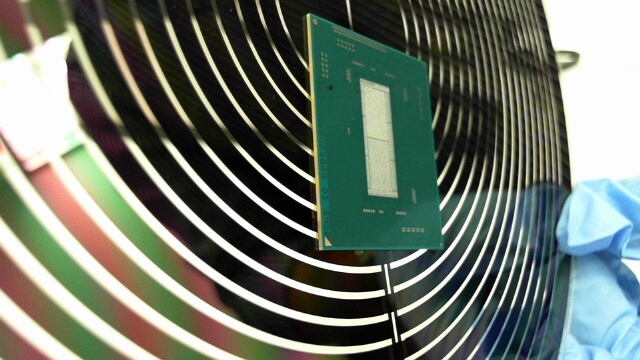
Instead, MESC bonding depends on coulombic attraction between a reusable carrier and the wafer or wafer coupon. The charge stored in an electrode embedded in the carrier induces an opposite charge in the wafer. The attraction between the two maintains the bond until the electrode is discharged. The required charge, a few thousand volts with only a few microamps of current, is far smaller and much more controlled than damaging ESD spikes. Charge monitor (CHARM) wafer testing found no changes attributable to the MESC system.
The bond is robust enough for most mechanical and thermal conditions the wafer might encounter and is inherently compliant. There is no adhesive between the carrier and the wafer, so differential thermal expansion does not induce stress. High-temperature carriers currently function at temperatures exceeding 450°C and can bond conductive, semi-conductive, and insulating materials. As the wafer expands and contracts, it simply slides on the carrier surface. Bonding and debonding are non-destructive to both the wafer and the carrier; carriers remain reliable for thousands of cycles over many years.

The MESC system works best with smooth, flat, conductive surfaces. It’s not limited to such surfaces, though, accommodating most wafers with consistent topography, such as an array of copper studs (the electrostatic bond is not suitable for aqueous processes, as capillary action allows liquid to infiltrate the space between the two surfaces). Reducing the amount of area in contact with the carrier generally reduces the strength of the bond, but varying the amount of electrostatic charge can often compensate for less-than-ideal surface characteristics.
Packaging customer use cases and applications are diversifying at a rapid rate, including reflow, plasma clean, flux clean, flip-chip, and various high-temperature cure techniques. Heterogeneous integration is forcing outsourced semiconductor assembly and test (OSAT) facilities to adopt new production techniques and the adoption of SEMI standards. A lack of standards for device handling and device interfaces has made it challenging for manufacturers to streamline production. There is a movement in the industry to move toward panels that are compatible with the ever-increasing interposer and device-size configurations.
Eshylon’s proprietary bonding technology has been proven in both wafer-level and custom-size trays and panel configurations. Carriers can be powered by onboard capacitance or even batteries. With integrated charging stations, carriers can be recharged or powered directly for more demanding process exposure conditions.
Due to the volumes required for large packaging facilities, Eshylon is working on a partnership with a large OEM that currently produces cutting-edge wafer-level and device automated handling equipment. Eshylon has developed a rack-mounted charge control module that interfaces with carrier charging units integrated directly into the pick-and-place tooling. This system will communicate directly to the main tool control and will have the ability to control multiple carrier charge units. This handling system will be able to change device bond strength and release on the fly, adjusting for varying substrate physical form factors.
Eshylon’s electrostatic carrier technology enables customers to run a broader spectrum of products through existing toolsets, reducing production tooling costs and improving overall yields. Taken together, these features make Eshylon Scientific’s handling systems for thin wafers and singulated devices a scalable, process-compatible alternative to adhesives and tapes.
This article first appeared in The 2021 Yearbook. View the issue here.