
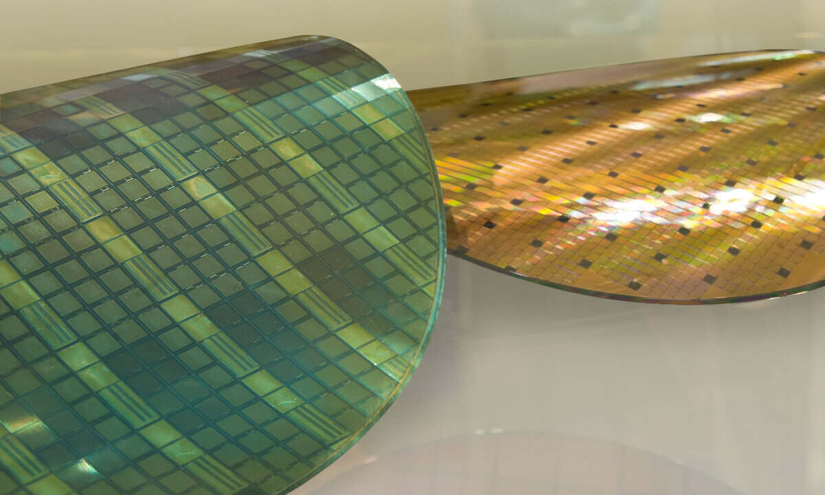
Temporary wafer bonding is widely employed in semiconductor device fabrication and in semiconductor device packaging applications, particularly now that changes in the Z dimension are calling for thinner and thinner silicon devices, and thinner and thinner packaged devices. This means that wafers and singulated die must be supported through parts of the fabrication and packaging processes by being temporarily bonded to some kind of sturdy carrier to prevent line yield losses resulting from mechanical stress of the wafers or the die.
We often think of using glue or other adhesives to stick objects together permanently, or temporarily, fixing one object to the other. But if the adhesive bond is to be used as a temporary means of fixture then we will need to deal with how to safely debond the objects without damaging them in the process. we will also need to deal with any residue that remains after debonding so as to not transfer adhesive residue to something else, or to avoid having the now debonded object stick again to something else.
The semiconductor industry, including the advanced packaging industry, has implemented commercially successful process flows for temporary bonding and debonding thin silicon wafers by optimizing the adhesive formulations used in bonding carrier-to-wafer, and subsequently debonding the two using approaches that involve combinations of heat, laser light, solvents, and various mechanical techniques. These adhesive-based (or polymer-based) temporary bond materials, and the equipment used to apply and remove them, are offered by a number of well-recognized companies, including 3M, Brewer Science, HD MicroSystems, EV Group, Süss, and others.
All of this is familiar territory to 3D InCites readers, surely, absorbed from conference presentations, the general literature, and personal experience with temporary wafer bonding materials and equipment.
A Novel Approach to Temporary Wafer Bonding
Readers, I like seeing fresh approaches that challenge conventional wisdom in novel ways. Which is why, during the recent Northern California Chapter of the American Vacuum Society 41stAnnual Equipment Exhibition and Technical Symposium, I was struck by the novel approach to temporary wafer bonding being exhibited by a company called Eshylon Scientific, based in Pleasanton, CA, not too far from the NCCAVS event in Milpitas.
Beyond the engineered tackiness of adhesives or polymeric materials being the basis for temporary bonding, there are other forces in nature that cause objects to come together and stick. Think gravity, for example. Objects with mass exert gravitational forces on other objects with mass, in proportion to their masses, and inversely scaling with the distance between the objects. We stick to the Earth as a result of gravitational attraction (most of it from Earth, but a little coming from us), and we cannot escape from the event horizon of a black hole, as a result of the massive gravitational field there, one strong enough to command galactic structures.
But, at least for now, we can’t turn gravity off.
What about magnetic force? Well, unlike gravitational force, which depends on mass, magnetic force depends on the magnetic properties of materials themselves, with some materials, generally metals, being highly susceptible to the influence of magnetic fields, while many other materials are not. Two strong permanent magnets will stick together if we orient the poles correctly (or repel each other if we don’t), but a strong permanent magnet will be useless sticking to glass. If we choose the material systems correctly, and if we use electromagnets rather than permanent magnets, we have a system we can turn on and off (bond and debond, so long as the objects respond to magnetic fields), with the bonding force being a function of how we energize and control the electromagnet(s).
Temporary Wafer Bonding using Electrostatic Force
And then there are electrostatic forces. Electrostatic action is the result of having two objects of opposite electrical charge attract each other over short distances; when the electrical charge for one of the objects is properly modulated, the sticking force can be directly controlled, subject to the material properties of the objects.
 We routinely manipulate electrostatic forces in semiconductor capital equipment to bond and debond (chuck and de-chuck, actually) wafers being processed in plasma etch tools, PVD systems, etc., equipped with electrostatic chucks. These ESCs pull wafers flat against the chuck, holding them firmly in place during the etch or deposition process sequences, and ESCs also permits direct control of wafer temperatures during energetic processing, as we see needed in plasma etching, for example.
However, these ESCs are fixed in place – wafers come to the process chamber, are placed on the de-energized ESC, are “bonded” by energizing the ESC, and then are debonded by de-energizing the ESC as the etch or PVD process terminates. The wafers leave, the ESC stays.
Eshylon Scientific’s idea is to combine the ease of electrostatic chuck bonding and debonding with already-established temporary wafer carrier technology deployed for thin wafer handling, bypassing adhesive and polymer bond materials with electrostatics.
That’s new, that’s interesting, and we recently spoke with Eshylon to learn more.
3D InCites: Please introduce yourselves and please give us a little bit of color on Eshylon Scientific.
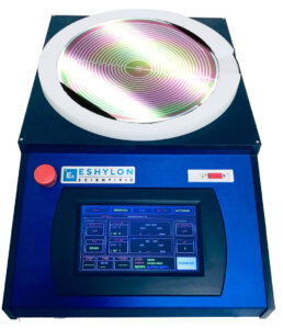
Eshylon: Thank you for the opportunity. Eshylon Scientific is a small group of folks who have backgrounds in the SEMI capital equipment space, nano-manufacturing analytics, and venture-backed small to medium-sized startups. Eshylon was founded in January of 2018 to help customers with their advanced and difficult handling applications with our new line of patented Mobile Electrostatic Carriers, which enable high yield, high throughput, low-cost temporary bonding with no clean steps and no use of chemicals.
3D InCites: Please help us understand more about your value proposition – i.e. the benefits of using mobile electrostatic carriers for thin wafer handling applications.
Eshylon: As the nano-manufacturing space continues to grow, there is a significant diversification of materials and process applications that generate new handling challenges in and out of modern-day production tooling. Most devices and sensors are built in layers of films on traditional silicon wafer sizes ranging from 100mm to 300mm. Customers need a solution to process thin materials, small pieces, new exotic materials, or anything that is outside of the standard wafer physical form factor. Our carriers enable our customers to expand the utilization of their existing toolsets without the addition of costly option upgrades.
 3D InCites: Would you explain to our readers please the “how” of your mobile electrostatic carrier system? What are the equipment components, how does the bond /debond process work, etc.?
Eshylon: Our current product offerings consist of a compact tabletop charging unit and a few variations of our “Predator” electrostatic mobile carrier design. The carriers are built on standard SEMI-specified silicon wafers using traditional nano-fabrication processes and materials. This ensures they will be compatible with the customer’s toolsets and process environments. Today, we manufacture our tabletop charging units at our facility in Pleasanton, California, and the carriers are manufactured at our foundry supplier in Campbell, California.

3D InCites: Cost of ownership (CoO) considerations are always critical to our industry’s enthusiasm for embracing new technology. CoO has many components, including capital costs, material costs, throughput, and yield, both mechanical yield and contamination-driven defectivity. What can you tell us regarding the CoO of your mobile electrostatic carriers compared to standard polymer-based temporary wafer bonding?
Eshylon:Beyond solving complex problems that other technologies can’t, CoO is where Eshylon’s carrier platform really shines. Our hardware cost of entry is a fraction of competitive systems, our carriers are completely reusable and as of yet have no measured limit to their useful life, and because we don’t use chemicals and there are no clean steps, there is no variable bonding cost, and our yield and throughput performance simply can’t be matched.
3D InCites: One of the problems we’ve run into in the past is being limited in processing temperature range when using polymer-based temporary wafer bonding. How’s the temperature performance envelope for your electrostatic carriers?
Eshylon: Our newest “Predator” carrier design includes an encapsulated secondary capacitor built with high-temperature materials. This ensures we can maintain our bond strength during high thermal exposure. We have successfully demonstrated functionality at process temperatures >500c.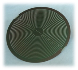
3D InCites: Ditto on materials – we may have a temporary wafer bonding process that’s optimized for thin silicon wafers, but we’d need to go back to the drawing board to port that process to other materials, for example, wide bandgap substrates like GaN or SiC. Or materials like glass.
Eshylon: III-V material handling currently represents our most significant area of growth. Most customers in this space approach us with a requirement for a solution to handle these materials on their lithography equipment. For example, a customer may have an ASML, NIKON, or equivalent exposure tool set up to process 200mm wafers. Most wide bandgap materials are only available at sized at or below 150mm. These smaller substrates can easily be temporarily bonded to our carriers for photoresist coating on the track and exposure on the litho tool. In many cases, the electrostatic carriers can then be implemented on other process steps such as etch and deposition.
 3D InCites: Where do you think the opportunities lie for your mobile electrostatic carrier solution to temporary wafer bonding?
Eshylon: As devices and process steps grow in 3D complexity, the need to temporarily bond, debond, and then re-bond again many times grows exponentially. We are currently focused on the lithography, etch, and deposition process steps, but have demonstrated capability on wafer thinning, ion-implant, etc. We are working on viable wet-processing solutions that are driven directly by customer demand. Today our solution is relatively manual working well for R&D and small volume production. Our strategy has always been to scale with an automated bond/debond tool which is currently in development.
3D InCites: Well we will certainly be on the lookout for that.
From Pittsburgh, PA, thanks for reading.
~PFW


