
The semiconductor industry is currently undergoing the most radical change in its history. Many new applications such as artificial intelligence (AI), augmented/virtual reality, and autonomous driving require enormous computing power with processors optimized specifically for each application. At the same time, development cycles are becoming shorter, costs for new chip designs are rising exponentially, and in many cases, yields are declining. All of these aspects can only be tackled if the principles of the entire semiconductor manufacturing process are changed.
While 2D transistor scaling is still important, the rising costs and complexity associated with scaling have driven the semiconductor industry to turn to 3D integration and heterogeneous integration — the manufacturing, assembly, and packaging of multiple different components or dies with different feature sizes and materials onto a single device or package — to increase performance on new device generations supporting these new applications.
This migration to advanced packaging as a leading driver of innovation began with the transition from monolithic to die-level systems, such as newly released smartphone application processors, which combine individual components such as the processor, memory, and AI/neural components using advanced packaging. This transformation will only accelerate in the coming years with the further miniaturization of these components from dies to chiplets, thus enabling a much more precise and individual mapping of customer and application requirements.
Chiplets and Hybrid Bonding
The ability to split large chips that are several hundred square millimeters into smaller parts can result in better yield, thus saving costs. Furthermore, only those chiplets requiring the latest-generation-node lithography have to be produced with that technology, whereas the remaining chiplets can be manufactured with older-generation (and less costly) lithography processes. Thus, the complexities and innovations of semiconductor manufacturing are becoming increasingly shifted into advanced packaging, which in turn makes flexible hybrid bonding technologies increasingly important.
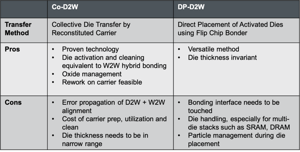
Wafer-to-wafer (W2W) hybrid bonding, which involves stacking and electrically connecting wafers from different production lines, is a central process in heterogeneous integration and has a proven track record of success for CMOS image sensors and various memory and logic technologies. However, since many chiplets are not necessarily the same size, a die-to-wafer (D2W) hybrid bonding approach may be a more practical option. There are several different D2W bonding approaches being considered for heterogeneous integration, each with different advantages and disadvantages as shown in Table 1. Determining which approach is best suited to a given application depends on several factors such as die size, die thickness, and total stack height as well as interface considerations such as contact design and density.
Collective Die-to-Wafer Bonding
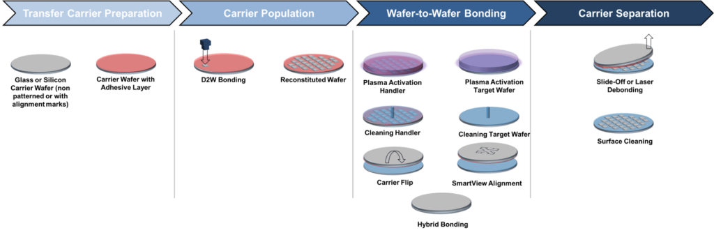
One hybrid D2W bonding method that has already been implemented in volume production for the past few years for applications such as silicon photonics is collective die-to-wafer bonding (Co-D2W). In Co-D2W bonding, singulated dies are transferred via a carrier wafer to the final wafer and bonded collectively in a single process step. The manufacturing flow for the Co-D2W bonding process is shown in Figure 1 and consists of four major segments: carrier preparation, carrier population, wafer bonding (temporary and permanent), and carrier separation.
Prior to the initial wafer dicing process, the wafer is coated with a protective layer to preserve the bonding interface quality during the dicing and pick-and-place processes as the bonding interface is orientated face-up on the dicing tape. The protection layer material can be a commercially available positive resist and/or any other protection layer that fulfills the specification of the dicing method used and can be subsequently completely removed using a solvent- or water-based cleaning process. The spin coating of the protection layer onto wafers with low topography can be performed using an EVG150 automated coating tool. For wafers with a topography that is greater than 5µm, spray coating can be performed using the same equipment.
To temporarily place the die on the collective die carrier using a pick-and-place D2W bonder and lock in their position during the cleaning, die preparation, and transfer process, the carrier wafer is coated with a commercially available temporary bonding material. The type of temporary bonding adhesive that is used depends on the post-processing steps and can be deposited on carrier substrates using the EVG850TB temporary bonder. Different metrology systems can be used during the carrier preparation process, such as the EVG40NT to measure die placement accuracy and the EVG50 to evaluate the incoming die height variation die-to-die surface planarity and the adhesive thickness.
The diced dies coated with the protection layer are placed with the bonding surface facing up on the collective die carrier to allow removal of the protection layer from the die surface. This removal can be accomplished using an EVG320 automated cleaning system using solvent-based and/or water-based cleaning chemistries.
In preparation for the hybrid bonding process itself, plasma activation in combination with deionized water-based wafer cleaning is used for substrate preparation on both the collective die carrier and target wafers. The carrier wafer is then flipped and aligned with the target wafer using an EVG SmartView NT optical aligner. Next, the dies on the carrier wafer are bonded with the target wafer using a GEMINI FB automated fusion wafer bonding system. Separating the collective die carrier from the transferred dies can then be accomplished using laser or thermal slide/lift-off debonding.
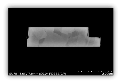
A recent publication highlighting this method demonstrated <2µm placement accuracy and high die transfer rate using currently available wafer bonding and debonding, die bonding, metrology, and cleaning process equipment.1 Figure 2 shows the transmission electron microscope cross-section images of the transferred dies after hybrid bonding. A closed bond line with Cu grains grown over the bonded interface could be demonstrated after subsequent thermal annealing. The Cu grain growth over the bonded interface indicates a high bonding quality. Further alignment improvements are expected with the next generation of die bonders, enabling the process flow to achieve well below 1µm overall die alignment accuracy.
Direct Placement Die-to-Wafer Bonding
Another hybrid D2W bonding approach that is beginning to be implemented for heterogeneous integration applications is direct placement die-to-wafer (DP-D2W) bonding whereby the dies are transferred to the final wafer one at a time using a pick-and-place flip-chip bonder. Figure 3 shows the manufacturing flow for the DP-D2W bonding process, which consists of three major segments: carrier population, die clean and activation, and direct placement flip-chip.
![[err-ad-fallback-title]](http://www.3dincites.com/wp-content/plugins/a3-lazy-load/assets/images/lazy_placeholder.gif)
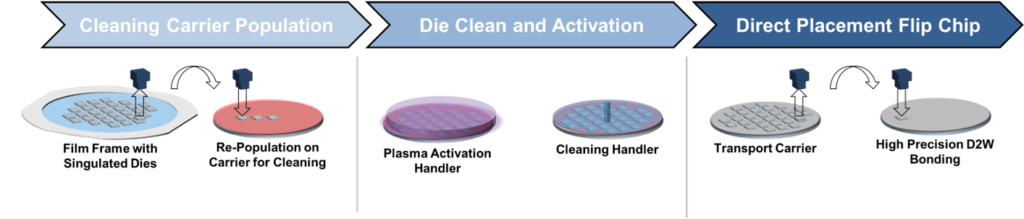
The DP-D2W bonding process flow begins much in the same way as the Co-D2W bonding process flow, with singulated dies added face up to a carrier wafer. Even though DP-D2W offers higher flexibility compared to Co-D2W, especially in terms of multi-die stacking for high bandwidth memory, the challenges in cleanliness and activation are the same as with any fusion bonding technique. In order to transport the wafers from the back-end grinding and dicing steps to a front-end clean hybrid bonding step, the dies often require repopulation on a dedicated cleaning carrier wafer. The carrier wafer then undergoes plasma activation and cleaning. However, instead of bonding the carrier wafer to the target wafer, the dies are bonded to the target wafer one by one using a pick-and-place flip-chip bonder.
The die cleaning step is a crucial part of the overall process flow that demands a dedicated tool for cleaning and activation. The recently introduced EVG320D2W has been designed as a highly flexible die preparation and activation system that features a universal hardware/software interface to enable seamless integration with third-party pick-and-place die bonding systems. It also can operate as a stand-alone system depending on integration and line balancing requirements. The system incorporates EVG’s advanced cleaning and plasma activation technology, which is available across its W2W fusion and hybrid bonding platforms and has been proven in hundreds of installed modules worldwide. It also features an integrated metrology module that provides direct feedback to the die bonder on critical process parameters, such as die placement accuracy and die-height information as well as post-bond metrology, for improved process control.
An Incubator for New Heterogeneous Integration Concepts
To determine the best bonding method for their respective devices, manufacturers must put together extensive development projects that not only take into account the wafer bonding equipment itself, but also the materials involved (such as photoresists and adhesives for temporary and permanent bonding), as well as related equipment and processes (such as wafer
cleaning, carrier handling, die bonding, etc.). Extensive process expertise is a must while having access to the latest-generation technologies is also key. However, since these systems are often already in production use at the customer’s site, they may not be easily accessible for R&D or experiments.
To address these challenges, EVG established the Heterogeneous Integration Competence Center™ (HICC), which assists customers in leveraging EVG process solutions and expertise to enable new and enhanced products and applications driven by advances in system integration and packaging. The basic idea for the foundation of the HICC is to make the barriers for development as low as possible to customers and to offer EVG as an incubator for new ideas. Through the HICC, EVG can assist in accelerating technology development, minimizing risk, and developing differentiating technologies and products through heterogeneous integration and advanced packaging all while guaranteeing the highest IP protection standards that are required for working on pre-release products.
Die-to-wafer Bonding Summary
D2W hybrid bonding is an enabling process to accelerate the deployment of 3D/heterogeneous integration and bring about new generations of devices with high bandwidth, high performance, and low power consumption. While the infrastructure for D2W hybrid bonding is still evolving, new process solutions and collaborations across the supply chain are on the rise and will play an essential role in creating the best-known methods of D2W hybrid bonding.
Acknowledgment
The author wishes to thank Jürgen Burggraf and Mariana Pires of EV Group for their assistance with the development of this article, as well as thank IRT Nanoelec and CEA-Leti for providing the substrates used in the CoD2W bonding demonstration cited in this article.
References
(1) J. Burggraf, M. Pires, T. Uhrmann, “Collective Die Bonding – An Enabling Toolkit for Heterogeneous Integration,” PRiME 2020 (ECS, ECSJ & KECS Joint Meeting), 2020.
This article first appeared in The 2021 Yearbook. Read the full issue here.